|
|
Bachelor's Degree in Telecommunications Systems and in Network Engineering. Bachelor's Degree in Aerospace Systems Engineering |
|
|
Laboratory 4: FSM and basic I/O Switches, digital inputs and outputs. FSM structure. Electrical bouncing and digital noise |
| 1. Specifications | Planning | Dev. & test | Prototype | Report |
We have two main goals for the laboratory session:
(1) read/poll digital input values and write digital outputs.
(2) study the software organisation of a typical application as a finite state machine (FSM).
|
|
|
Fig. 1. Example circuit for reading inputs and writing outputs. |
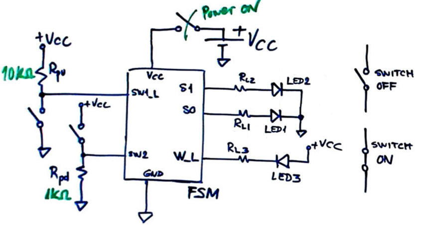
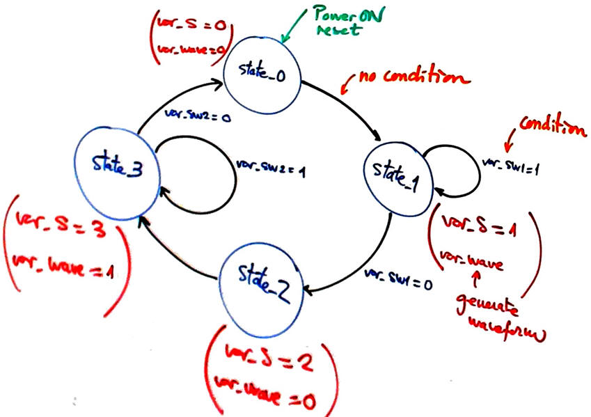
Our circuit will read (poll) two switches and perform the state diagram represented in Fig. 2. Two active-high LED are wired for indicating in binary the state that the FSM is executing: "00", "01", "10", "11". Another active-low LED connected to W_L will generate a 12 Hz square wave.
|
|
|
Fig. 2. Example circuit for reading inputs and writing outputs. |
Circuit features using a bullet list:
Accordingly to the state diagram the machine has these three operating modes:
- SW1 = SW2 = '0': the FSM is jumping freely from state to state. In this way the W_L output will be a 75% duty cycle rectangular waveform the frequency of which will be determined by software execution times.
- SW1 = '1': the FSM generates a 12 Hz square waveform.
- SW2 = '1': W_L = '0' and so the LED3 is always ON.
NOTE: Important concepts for our introduction to programming μC: bare metal vs. RTOS vs. OS (1), (2)
Topics in EMC
How to protect digital inputs? This is a reference to start with this important issue.
Find and discuss analogue and digital methods for reducing the signal bouncing associated to mechanical switches. Find examples in real schematics or commercial chips. An interesting link: (1).
These are general ideas on PCB and EMC: de Mendizabal, I., The 10 most common EMC challenges in a PCB design, All about circuits magazine, 2024.
| Specs | 2. Planning | Dev. & test | Prototype | Report |
Hardware
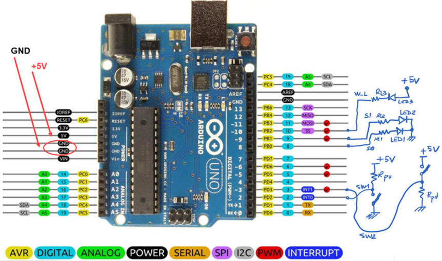
In this introductory application planning the hardware means simply thinking about where to connect switches and LEDs to Arduino pins. We can power the application from the USB +5V connector or from the external unregulated +Vin plug.
|
|
|
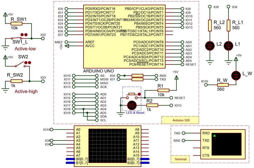
Fig. 3. Hardware circuit for selecting I/O pins. Light blue labels show the pins that can be configured as digital inputs or outputs in this typical AVR microcontroller ATmega328P populating the Arduino UNO board. |
Software
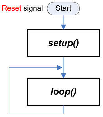
Software running in Arduino or other similar training boards will be organised in two main parts. A system initialisation function setup(), and an infinite loop that executes continuously loop(). A high-level C-like Arduino compiler will be used to generate the assembly language executable file.
|
|
Fig. 4. Software flowchart. Setup() configures the system and loop() contains the assembly code to be executed continuously at the maximum microcontroller speed. |
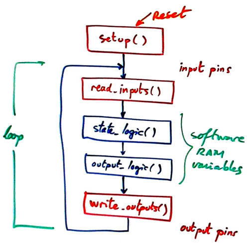 |
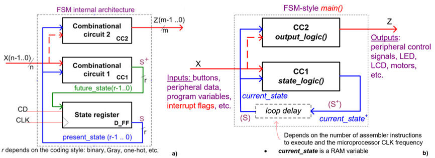
Software programming style for solving all laboratory applications will be based on the architecture of a finite state machine (FSM). We adapt the typical FSM architecture from digital systems to computer programming replacing the state register based on data flip-flops by a RAM variable updated every time that the loop is executed.
The fundamental idea of synchronicity derived from the CLK signal will be discussed in next laboratories.
|
|
|
Fig. 4. a) FSM architecture using digital circuits. b) FSM adapted to computer programming. |
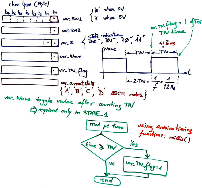
The way for generating a squared wave when at STATE_1 will be simply toggle the variable var_Wave after having measured a period of time TW = 41.6 ms. All the RAM variables will be char (byte) type for easy debugging using the watch window.
|
|
|
Fig. 4. List of RAM variables. Arduino timing functions such millis() will be used for measuring timing periods. |
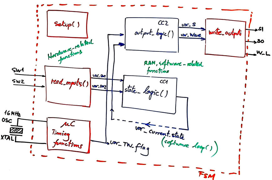
The application can be conceptualised using our hardware/software diagram represented in the next Fig. 5. The advantage of such organisation is the separation of hardware-related interface functions and pure software functions independent of the hardware that are processing RAM memory variables.
|
|
|
Fig. 5. Hardware-software diagram. |
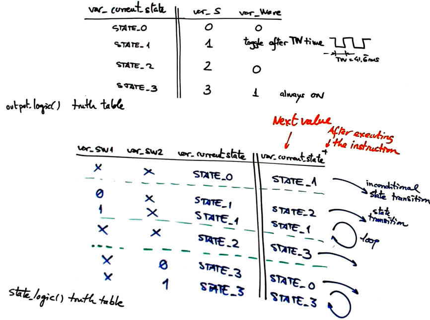
Our circuits' truth tables are solved executing software routines.
|
|
|
Fig. 6. Truth tables for the state_logic() and output_logic() combinational circuits. |
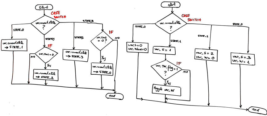
As shown in Fig. 7, before obtaining the C code for each truth table, we will draw the equivalent flowchart interpretation where the corresponding statements are easily identified.
|
|
|
Fig. 7. Interpreting the truth tables as flowcharts for ready for translations into C code. |
Simulation project location:
C:\DEE\LAB4\Proteus\(files)
Prototype and PCB project location:
C:\DEE\LAB4\PCB\(files)
| Specs | Planning | 3. Dev. & 4. Test | Prototype | Report |
Hardware
The first step consists in capturing the schematic in Fig. 1 in Proteus. This is the FSM.zip file containing the hardware (FSM.pdsprj) and software (main.ino) project files.
|
|
Fig. 8. It is a good idea to simulate the application and run and test for debugging purposes. This picture shows the circuit capture in Proteus. |
Software
The idea is to start adapting a similar example. All our applications will consist of FSM architectures. This lab itself becomes an example to copy and adapt. Using the simulator it is possible to run and follow in detail the code execution while interacting with hardware devices.
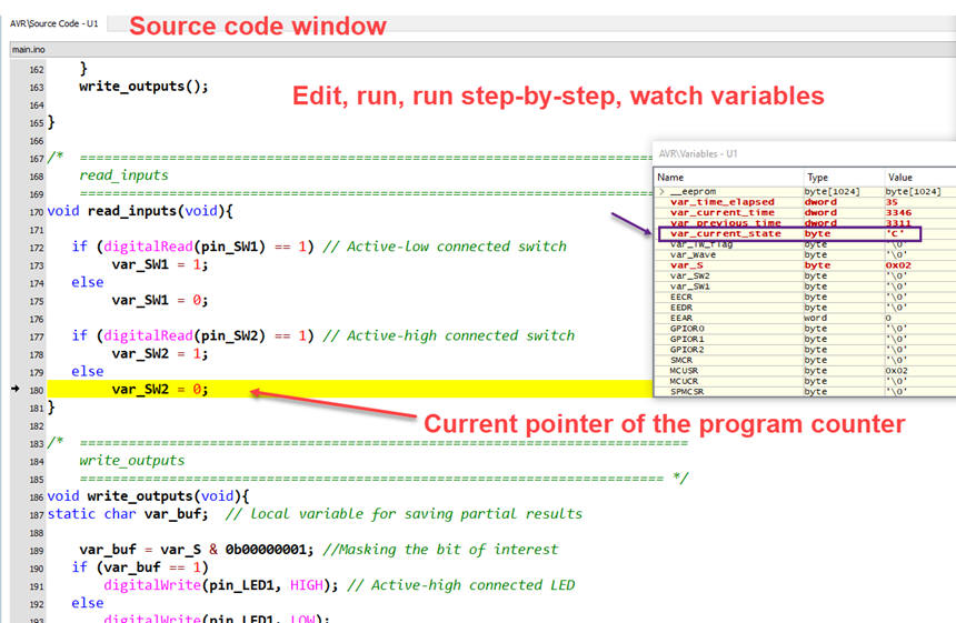
Explain how the switches are read and how the output pins are written. Use step by step mode, add a watch window to monitor the circuit's RAM variables.
|
|
|
Fig. 9. Source code that can be edited from the Proteus window itself. |
Capture signals using the logic analyser.
|
|
|
Fig. 10. Instruments and watch window for debugging purposes. |
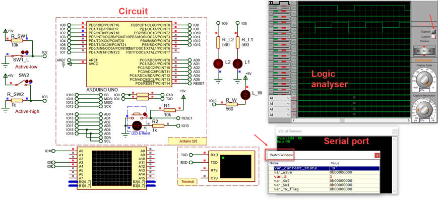
NOTE: Print logic analyser results using the PDF format and setting white background to save ink.
Additional ideas to study and characterise the circuit:
- Measure the frequency of the signals generated using cursors and also the frequency meter instrument.
- Modify the code (FSM.zip) so that a new fsm() function with a single switch-case replaces state_logic() and output_logic().
- Modify the state diagram so that timing functions such millis() to generate the 12 Hz waveform are used only when SW1 = '1' (FSM.zip). Keep the same 75% duty cycle rectangular waveform at W_L pin. Measure its frequency when SW1 = '0', SW2 = '0'.
- Modify the state diagram so that SW1 has priority over SW2.
| Specs | Planning | Dev. & Test | 5.Prototype | Report |
Protoboard or universal PCB breadboard
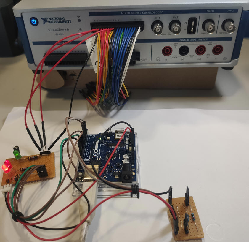
Download the application to an Arduino board and build the circuit in protoboard or universal PCB as in LAB3. Perform measurements using VB8012 logic analyser instrument to characterise this design and observe how the FSM is switching states accordingly to the read values from switches.
|
|
|
Fig. 11. Prototype running. |
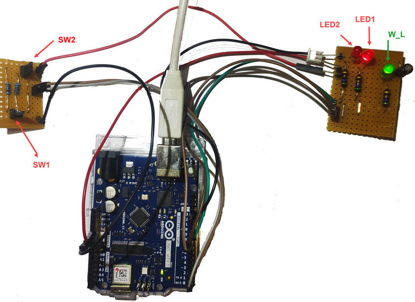
Fig 12 shows connections to the VB8012 logic analyser instrument.
|
|
|
Fig. 12. Connecting digital signals of interest to the VB8012. |
|
|
|
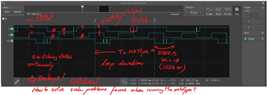
Fig. 13. SW1 = SW2 = '0'. Capturing waveforms and visualising real phenomena. Logic analyser running at 1 GS/s. |
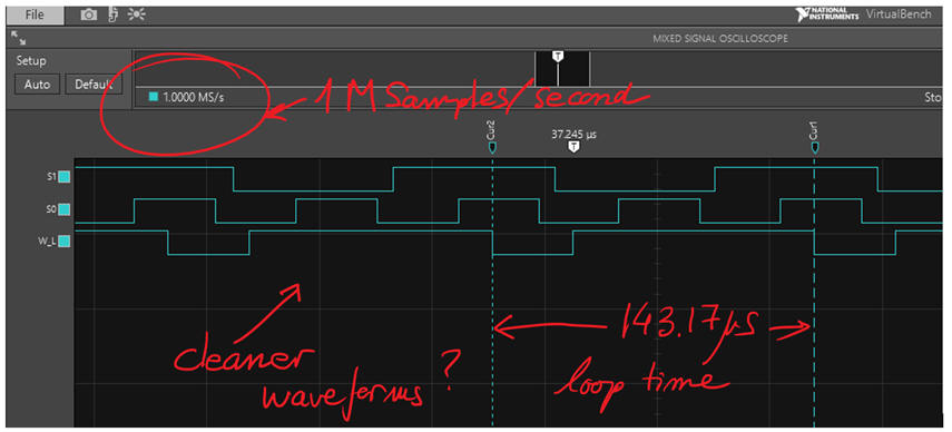
Why when sampling at 1 MS/s (Fig. 14) the captured waveforms are cleaner and the glitches do not appear? Thus, which one is the real waveform generated by the prototype circuit?
|
|
|
Fig. 14. SW1 = SW2 = '0'. Capturing waveforms and visualising real phenomena. Logic analyser running at 1 MS/s. |
In Fig. 15 we see the output W_L generating the expected 11.8 Hz squared signal.
|
|
|
Fig. 15. SW1 = '1'. Capturing W_L. The FSM is running only in STATE_1 generating the squared waveform. |
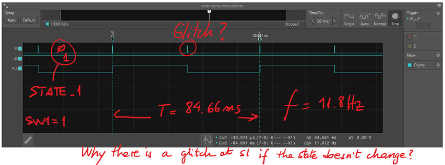
We can discuss solutions to eliminate such undesirable or unpredicted effects such delays and glitches. How software can be improved? What is the significance of 7.5 ms delays and even shorter glitches of 7 ns in this application?
PCB in KiCad
At this point it is useful to introduce the idea of the Arduino shield PCB for prototyping using connectors. The idea is to avoid wires and make robust prototypes.
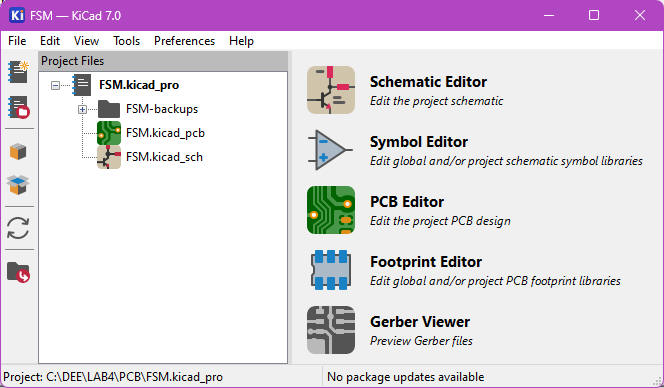
This is the KiCad introductory project: FSM_PCB_KiCad.zip. LAB4 is aimed as a tutorial for easing the learning curve for such time-demanding EDA tools. Thus, there is no need to start any other project from scratch. As which all the other project sections, LAB5 prototype will be an adaptation from this one.
|
|
|
Fig. 16. KiCad project window. |
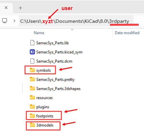
NOTE: Current CSD and DEE KiCad symbols, footprints and 3D tuned components are available in these three libraries: symbols.zip, footprints.zip and 3dmodels.zip, to be unzipped and placed in the corresponding 3rdparty user directory. Basically, in this introductory level the idea behind tuning components is to enlarge their pads for easy soldering.
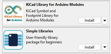
Other third party libraries are available installing plugins. As shown in Fig. 17, the library manager menus are accessed clicking the preferences top tap.
|
|
|
Fig. 17. Global user libraries with some components from this LAB4. Other third party libraries are also easily installed from the plugin and content manager. Specially recommended are the Simple Libraries for beginners and also the KiCad Library for Arduino Modules. |
Open the project FSM.kicad_pro. Fig. 18 shows the schematic capture. As previously in Proteus simulations, many symbols are used to translate and capture the sketch.
|
|
|
Fig. 18. Circuit capture FSM.kicad_sch. |
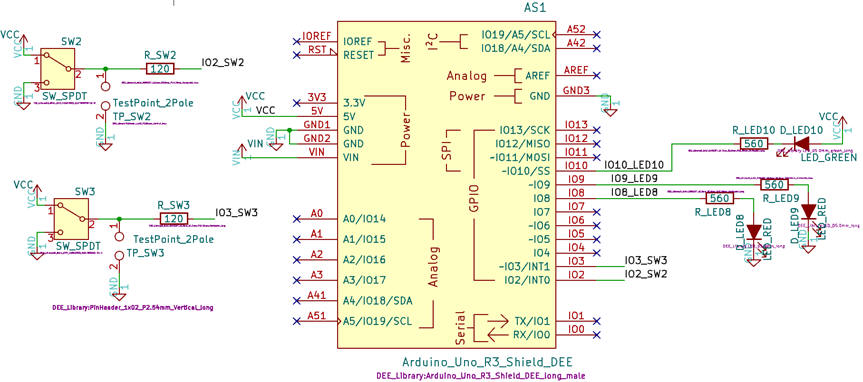
Fig. 19 shows how the components are placed on the PCB before routing tracks. Components from the schematic must have attached a footprint. Examine the libraries to find them. You can easily add new footprints copying and adapting from other similar ones. Many times vendors and component distributors have also available footprints for several component cases.
|
|
|
Fig. 19. Example component placing in an Arduino shield before routing. |
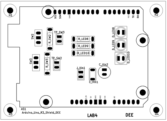
Fig. 20 shows the picture of the bottom layer. Basically, at this introductory level, nets are divided in two two main classes: default and power. This picture shows power nets routed with 2 mm width and all the other default nets at 1 mm.
|
|
|
Fig. 20. Bottom layer from the FSM.kicad_pcb where most of the tracks are routed. |
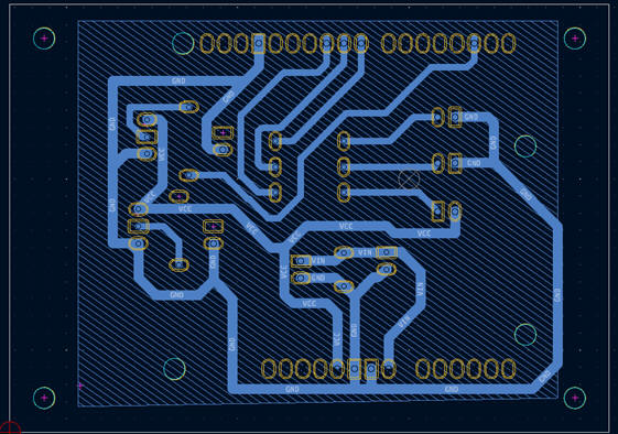
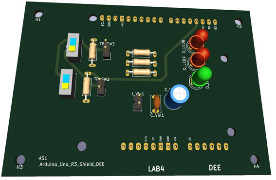
Fig. 21 shows the top 3D view of the Arduino shield. Here is where the 3D models are required. As with the footprints, 3D models for many components are available or may be designed using FreeCAD.
|
|
|
Fig. 21. Top 3D view. |
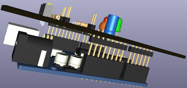
3D models can be quite complex and realistic looking. For instance Fig. 22 shows how to attach the Arduino shield to the Arduino UNO R3 3D model.
|
|
|
Fig. 22. Top 3D view. |
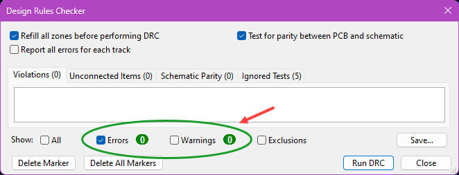
PCB may be finally validated when from both paired schematic and PCB views there are no errors or warnings. Fig. 23 shows the electrical rule checker (ERC) window.
|
|
|
Fig. 23. Electrical rules checker (ERC). |
The final aim of PCB EDA tools is to render Gerber files for PCB machinery and be able to manufacture the prototype.
This project may be continued mechanising the box using 3D printing software.
Alternatively, other similar EDA tools can be used for prototyping PCB and simulation. For instance, Multisim + Ultiboard from National Instruments. This is the same LAB4 project FSM_PCB.zip.
Experimentation and measurements
| Specs | Planning | Dev. & Test | Prototype | 6. Report and post-lab assignments |
Your report should look like this web page, organised in five sections.
IMPORTANT NOTE: Print logic analyser results and simulator graphics using the PDF format and setting a white background to save ink. In this web format, pictures can also be represented in black background, but it is not possible when preparing materials for printing in paper.
NOTE: Print file listings in sheets of paper using your printer or our UPC printer system as coloured annexes using the indicated tools. Once printed, comment the code lines of interest using handwriting or electronic ink.
Generate a new project FSM2 adding a new switch SW3 to choose between two rectangular output waveforms: 30% DC when SW3 = '1', and 75% DC when SW3 = '0'. Project location:
C:\DEE\LAB4\FSM2\(files)
Write a report discussing only the hardware and software adaptations and changes with respect this tutorial FSM project.
| Home Contact Tutorials Electronic devices and companies Books Magazines Instruments Digsys Library EETAC DEEL |

|
|
| Web activa des de 01/2023, @ F. J. Robert. Web editat amb Microsoft Expression Web 4. El contingut és material de referència per al disseny d'equips electrònics. Llicència:Reconeixement 4.0 Internacional de Creative Commons |