|
|
Bachelor's Degree in Telecommunications Systems and in Network Engineering. Bachelor's Degree in Aerospace Systems Engineering |
|
Laboratory 5 Buttons, keyboards, events and interrupts. FSM structure and CLK synchronisation. |
The main goal of this laboratory is to enhance the FSM architecture to handle interrupts. We can easily conceive simple projects such:
Project #1: Modify the previous FSM tutorial in Lab4 adding a button ST.
Project #2: Design a LED blinker using Arduino
|
Project #1: Lab4 adding a button ST. |
| 1. Specifications | Planning | Dev. & test | Prototype | Report |
(1) Modify the previous FSM tutorial in Lab4 adding a button ST. The FSMI is kept idle until ST is clicked two consecutive times, and it works continuously until another click is detected.
(2) Add a flag variable to write ASCII messages to the serial port, so that it can be used for monitoring FSM operations.
|
|
|
Fig. 1. Basic application FSMI enhanced with external interrupt detection. |
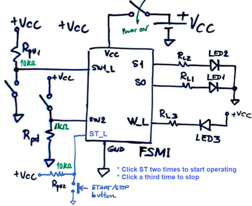
We will add hardware components and modify the state diagram so that the application will work as specified.
|
|
|
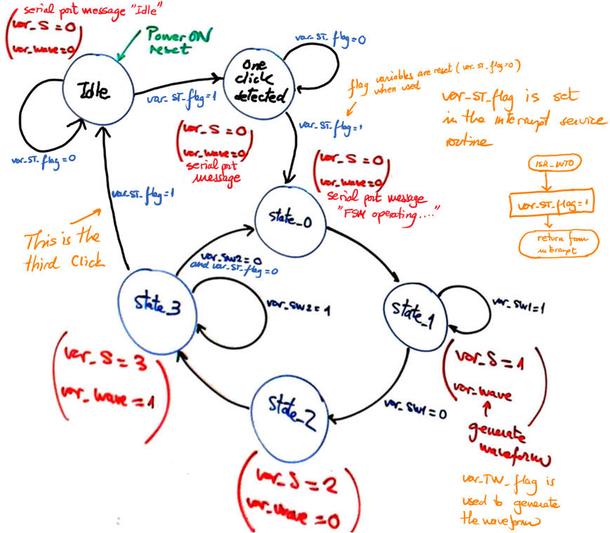
Fig. 2. Proposed modifications in the state diagram. |
Topics in EMC
Bouncing and noisy signals associated to mechanical push-buttons complicated the acquisition and detection of signal edges or logic transitions. Measure and characterise this event using the VB8012 instrument. We need to experiment with the prototype to visualise waveforms on the oscilloscope and check if button click events are correctly sampled.
Find examples on debouncing circuits. What is the typical button debouncing hardware and software solution found in books and examples? Study these materials in Debouncing_filter.
| Specs | 2. Planning | Dev. & test | Prototype | Report |
Our goal is organise the application software as a finite state machine (FSM) taking advantage of that we already learned in LAB4. The state diagram will be sensitive to the detection of external interrupts events.
Hardware
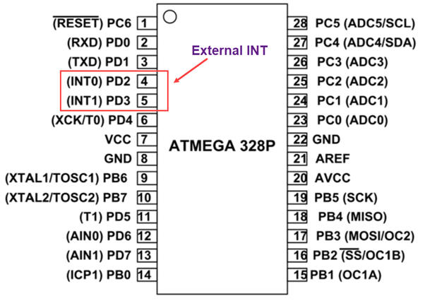
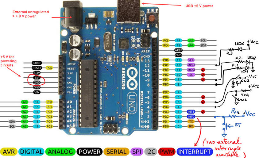
The chip ATmega328P allows two external interrupt sources INT0 and INT1 wired at Arduino pins 2 and 3 respectively. Thus, we will relocate the other switches and LED as indicated in Fig. 3 to other unused pins.
|
|
| Fig. 3. The ATmega328P microcontroller is the core of the Arduino board (picture ref.). Pin 2 of the port D (PD2) named Arduino digital pin 2 is also INT0, where an external push button is connected to trigger interrupts. |
Software
Software will be upgraded to consider external interrupt acknowledgement. The interrupt service routine ISR() (or he interrupt handling routine), will be installed dynamically in setup() function as recommended in the reference manual.
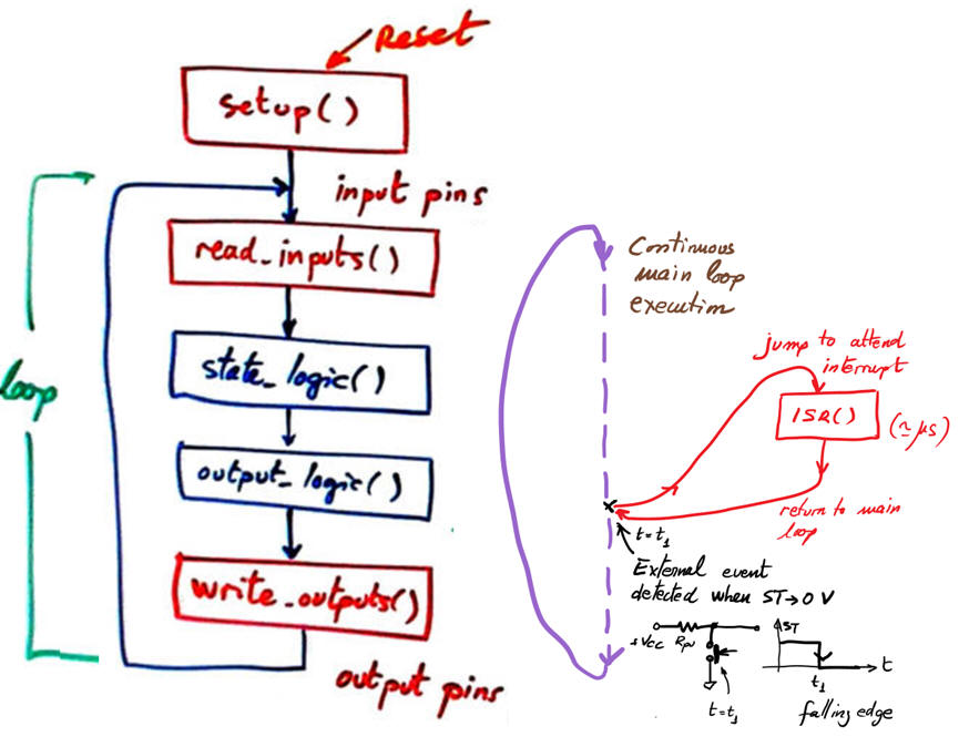 |
Fig. 4. The microcontroller allows the fundamental idea of jumping to the interrupt service routine exactly when the event, this time an external button click, happens. We will use the ISR() simply to set a software var_ST_flag to control the FSM as we do with others RAM variables. |
We will use the ISR() simply to set a software var_ST_flag to control the FSM as we do with others RAM variables. This ideas are well represented in the hardware-software diagram in Fig. 5.
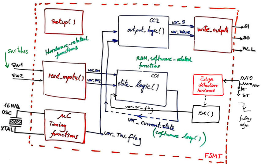 |
Fig. 5. Hardware-software diagram introducing the extra function to attend interrupts. |
RAM variables and the structure and organisation of the remaining functions are inherited from Lab4.
Simulation project location:
C:\DEE\LAB5\Proteus\(files)
Prototype and PCB project location:
C:\DEE\LAB5\PCB\(files)
| Specs | Planning | 3. Dev. & 4. Test | Prototype | Report |
Hardware
We can inherit all previous Lab4 project and rename it. This is the FSMI.zip file containing the hardware and software project files. Open Proteus and run the application.
|
|
|
Fig. 6. Proteus captured circuit running interactively while watching variables. |

Software
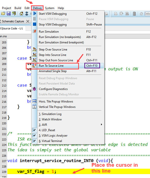
While debugging, we can use "Ctrl+F10" to stop the code execution exactly in the interrupt service routine to check that this vectored jumping mechanism works correctly.
|
|
|
Fig. 7. Stopping the execution at a given line of code. |
Measure the maximum W_L waveform frequency when SW1 = SW2 = '0'.
|
|
|
Fig. 8. Example of waveform capture from the logic analyser instrument. |

| Specs | Planning | Dev. & Test | 5. Prototype | Report |
Protoboard or universal PCB breadboard
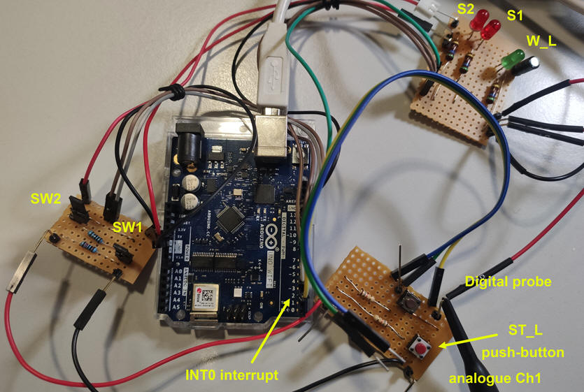
We use the previous circuit and solder a button ST_L to connect it to the Arduino pin 2 (INT0). We upload the executable file (hex) to the platform using Proteus or Arduino IDE.
|
|
|
Fig. 9. FSMI running. |
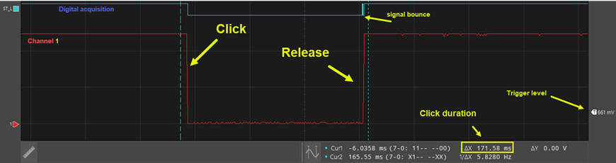
The prototype allow us to perform several measurements and observe the behaviour when clicking push button. For instance, Fig. 10 shows the acquired analogue and digital signal for a short click event.
|
|
|
Fig. 10. Short click event about 200 ms |
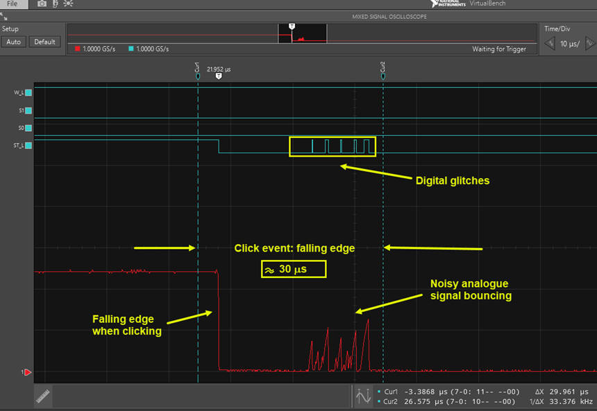
As shown in Fig. 11, many times and randomly, digital noise or glitches are generated when clicking, and they can make the FSM to malfunction.
|
|
|
Fig. 11. Signal bouncing for 30 us on the ST_L button falling edge when clicking. |
How to generate clean digital signals and filter out all electrical noise?
PCB in KiCad
We can use the previous LAB4 template and add the new elements, basically the push-button, reassign some inputs to be able to connect INT0 to the ST_L button. This is the FSMI_PCB.zip file in KiCad.
NOTE: Current CSD and DEE KiCad symbols, footprints and 3D tuned components are available in these three libraries: symbols.zip, footprints.zip and 3dmodels.zip, to be unzipped and placed in the corresponding 3rdparty user directory. Basically, in this introductory level the idea behind tuning components is to enlarge their pads for easy soldering.
 |
|
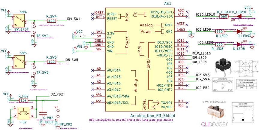
Fig. 12. Schematic in KiCad. |
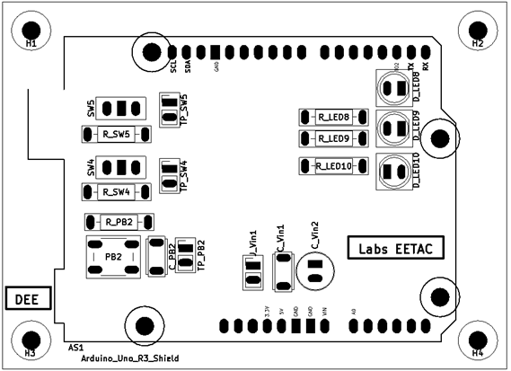
You can route and complete the PCB represented in Fig. 13.
 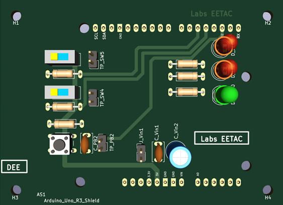 |
|
Fig. 13. Picture of PCB component placement and top layer in KiCad. |
This is yet another version of the prototype shield using the EDA tools Multisim and Ultiboard FSMI_PCB.zip.
Experimentation and measurements
| Specs | Planning | Dev. & Test | Prototype | 6. Report and post-lab assignments |
We propose a new project to introduce the CLK signal concept for synchronising FSM state transitions as in a conventional sequential circuit and being able to obtain accurate waveforms. The application symbol is represented in Fig. 1: let us design a 3-bit binary counter synchronised with an external 10 Hz signal, with code selection (Code), count enable (CE) and terminal count detection (TC8) that is set when at the last state.
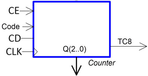 |
Fig. 1. Counter's symbol. Write the function table and a timing diagram. |
- Switch Code = 1 radix-2; Code = 0 Gray.
- Switch CE = 0, disabled; CE = 1, count enabled.
- CLK external rectangular or squared 10 Hz signal.
- CD is the mC reset button.
Hardware variations: Add another red LED to the board to visualise Q2..0). Use the green LED as TC8.
Propose an state diagram as in Fig. 14 for this application and solve the project.
|
|
|
Fig. 2. Example of state diagram and the solution for the state and output logic truth tables. |
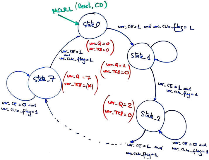
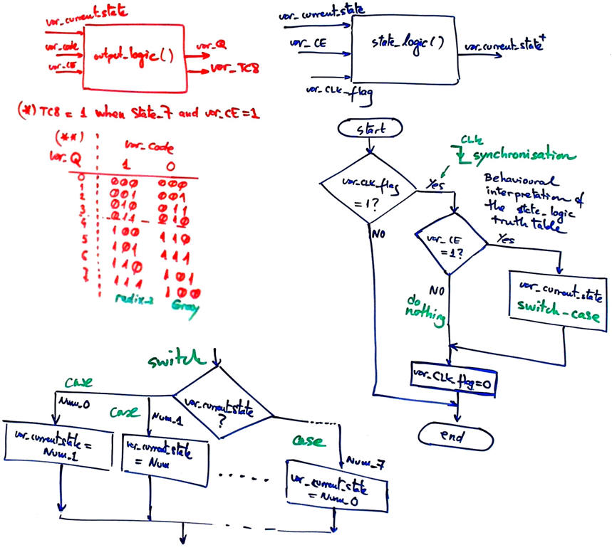
Fig. 3 shows an example of hardware schematic in Proteus ready for simulations.
|
|
|
Fig. 3. Circuit running in Proteus. We can drive the CLK signal clicking a button or connecting an oscillator. |
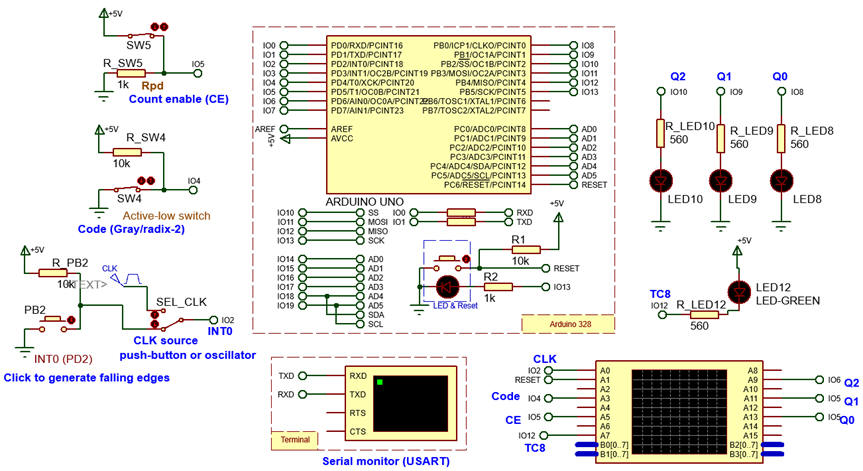
Solution example Counter.zip in Proteus. Use KiCad and modify the PCB to suit this application. Consider a two-pin header for connecting the CLK square wave generator selected with the CLK_source switch.
| Home Contact Tutorials Electronic devices and companies Books Magazines Instruments Digsys Library EETAC DEEL |

|
|
| Web activa des de 01/2023, @ F. J. Robert. Web editat amb Microsoft Expression Web 4. El contingut és material de referència per al disseny d'equips electrònics. Llicència:Reconeixement 4.0 Internacional de Creative Commons |