|
|
|||||
Chapter 1 problems |
- D1.14 - |
9-bit parity generator and parity checker |
|||
|
|
|||||
1. Specifications
The project objective is to design a parellel 8-bit data transmitter and receiver system TX_RX_9bit with parity bit generator and checker, hence, a nine bit parallel system. Fig. 1 shows an initial sketch of the the idea. We will be able to select which parity to use: odd or even.
We will also implement a transmission channel simulator so that we can toggle the value of anyone of the nine transmitted bits, imagining that some kind of noise or interference has flippled the value of a single bit.
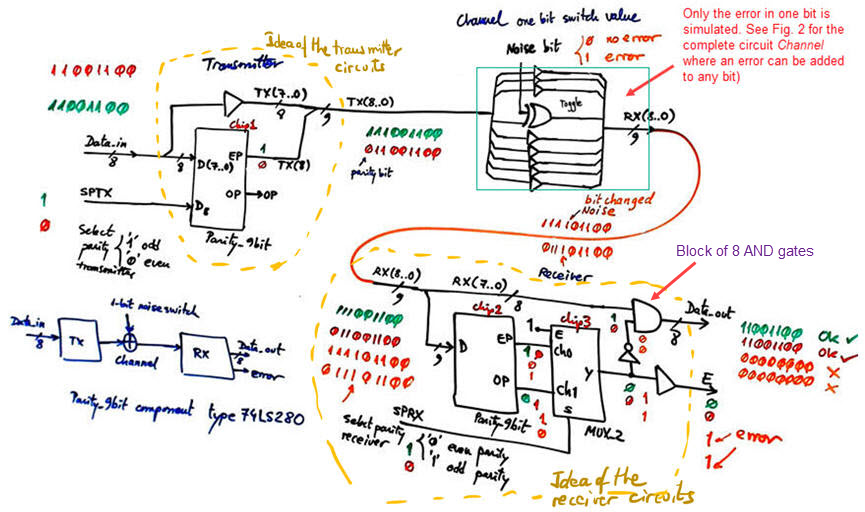
The circuit relies on the component Parity_9bit practically identical to the standard type SN74LS280 to be implemented as a component in VHDL and other devices from previous projects. Transmission channel induced errors of 1-bit can be simulated using a XOR gate. When the data received is wrong (meaning wrong parity) an Error flag is generated and the received byte is reset because it is of no use (the transmitter must resend the data). Implement and test the system in VHDL using plan C2.
The same project B3.14 is proposed in Chapter 3 for learning the basics of μC software organisation and basic digital I/O.
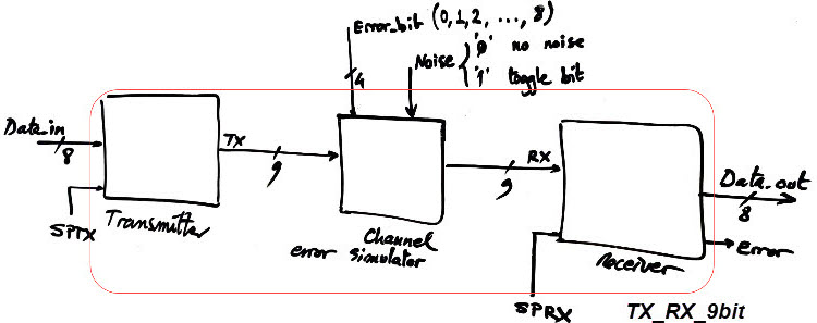  |
|
Fig. 1. An sketch on the idea of the circuits that may include our system TX_RX_9bit: 8-bit parallel transmission system with an additional ninth parity bit. Apply several Data_in vectors selecting a given parity to see how it works. The initial channel simulator shows how to flip or toggle a single bit value using a XOR gate (TX5.). A complete channel simulator where the noise can be added to any one of the 9 bits is presented in the next Fig.2. |
Fig. 1 sketch shows that only TX5 is affected by error. We can generalise this channel model using logic blocks from P2. Thus, the idea of the transmission channel simulator to allow us to modify the value of any of the nine bits is shown below in Fig. 2. Explain and check whether the circuit proposed is right and can be used for adding noise to any wire.
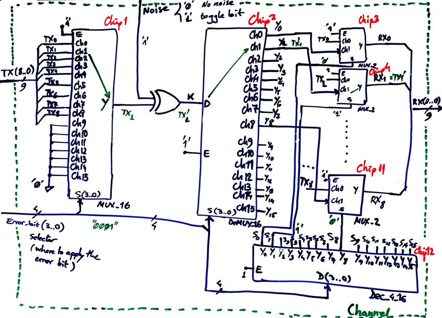 |
| Fig. 2. Tranmission Channel simulator to introduce tranmission errors for testing the equipment. Error_bit(3..0) vector select to which bit the inerference is added. |
For instance, Fig 3 shows an implementtion using plan A of the chip SN74LS280 truth table. In this way, the chip Parity_9bit as used and represented in the transmitter and also in the receiver, is simply this chip connecting Even --> OP and Odd --> EP outputs.
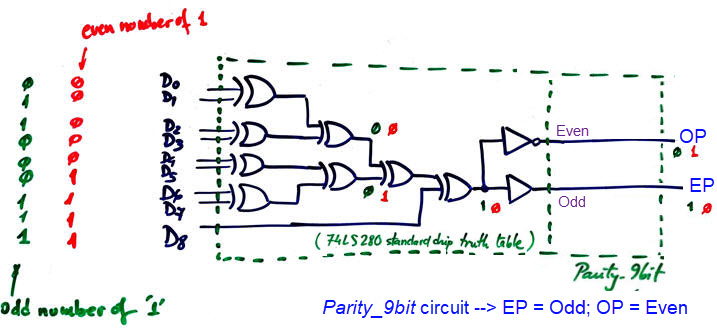 |
| Fig. 3. Example plan A equations implementation for the 74LS280 standard component (9-bit odd/even parity generators/checkers). The even and the odd parities of the 9-bit incomming data are detected. If the number of ones is even (0, 2, 4, 6, 8) Even = '1', and thus EP = '0'. |
PLA3 specifications include: symbol, truth table, data range, example commercial chips with similar functionality, etc. You may like to add theory to better explain and comprehend these circuits.
Draw the testbench fixture and an example of timing diagram to be used later as stimulus in the VHDL verification of the synthesised circuit. Consider Min_Pulse = 77.8 ms. You can use as example test vectors for the Data_in input one of the following options ('0x' means Hexadecimal, '0b' is radix-2, thus 0x6F = 0b01101111. Add more numbers if you like it.
-
Option #1: 0x6F, 0x02, 0xC3, 0b10101011, 0xC3, 0b00100011, 0x5D, 0x77
-
Option #2: 0x75, '0x2A, 0b00101010, 0xC9, 0b11101111, 0x33, 0x00, 0xFF
-
Option #3: 0x45, 0x3B, 0b00111011, 0x6C, 0x75, 0xFA, 0b00000001, 0x7C
If we liked to test all the circuit, how long would it take to run the full verification?
This system simply allows the detection of a single bit error. Study the idea behind Hamming codes for not only detecting but also correcting transmission errors, for instance the Hamming (7,4) and how to design a circuit to implement such algorithm.
CPLD or FPGA target chip options:
Target option #1: MAX II
Target option #2: Cyclone IV
MAX10 chips are not used because Intel Quartus does not generate the "*.sdo" file for running gate-level simulations.
Additional specifications for PLA4_1 for performing timing simuations and measurements:
Calculate the propagation delay in a given signal transition using gate-level simulations in VHDL.
Calculate the circuit's longest propagation delay and maximum speed for a given target chip using the timing analyser tool.
If we liked to test all the circuit, how long would it take?
Be aware that the location of this project enhanced with timing simulation and measurements (section 5) is:
C:\CSD\P4\TX_RX_9bit\(files)
This transmission system can be serialised in P7 and P8 using synchronous shift registers, as shown in the tutorial USART.
2. Planning
Invent the plan C2 schematic for this TX_RX_9bit.
Project location:
C:\CSD\P3\TX_RX_9bit\(files)
These are proposed option for some internal components also using plan C2:
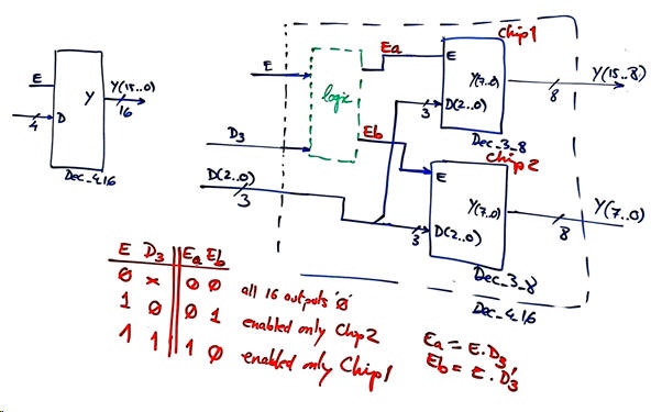
Dec_4_16:
-
Option #1: Expanding components Dec_3_8 (designed internally using plan B)
For instance, this sketch below is an initial idea on decoders exapandability.
-
Option #2: Expanding components Dec_2_4 (designed internally using plan A)
-
Option #3: Expanding components Dec_1_2 (designed internally using plan A)
In the reocording DT2.5 there is a Dec_3_8 build using smaller Dec_1_2.
DeMUX_16:
-
Option #1: Expanding components DeMUX_2 (designed internally using plan A)
-
Option #2: Expanding components DeMUX_4 (designed internally using plan A)
-
Option #3: Expanding components DeMUX_8 (designed internally using plan B)


