| | ||
PLA4.1: Gate-level and timing analyser simulation measurements |
||
| NOTE: Learn how to perform gate-level simulations and how to measure using the timing analyser in this Lab4.1. This post lab assignment PLA4 must be solved only after having completed successfully the lab session; it consist in repeating all the concepts in another similar circuit. |
Specifications
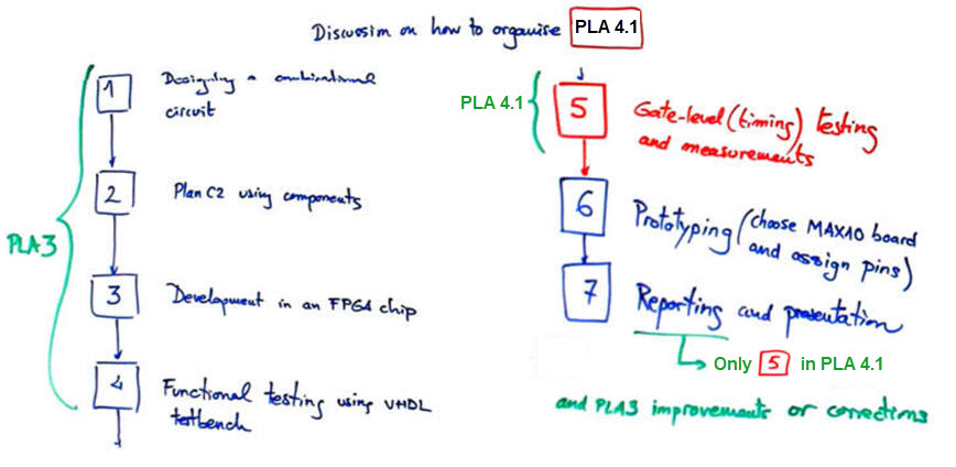
We will continue the project proposed in PLA3 developing the new VHDL design flow step #5: characterising how fast is the circuit for the given internal design architecture you solved in PLA3, and for a given target chip option.
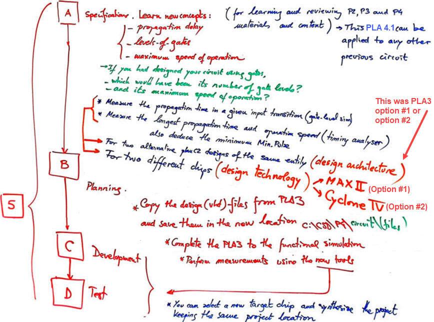
This PLA4 is also a project in itself, as all the others, so plan it using several sections like A, B, C, D. The main theory content related to this PLA is in lecture L4.3.
You can use in gate-level simulations the same PLA3 testbench fixture and its VHDL file that were used in functional simulations.
Initial work:
Solve Lab4.1 in your computer to learn gate-level simulations and timing analyser tool.
If your PLA3 circuit is not yet fully operational or were not correctly synthesised or tested, take some time to correct it. PLA3 sections 1-2-3-4 do not have to be reported again, explain only in an annex what was wrong and corrected. If your PLA3 is fully operational, perform more operations in binary, explain better the operands, results and flag.
Print and comment the technology view that now will be tested in this design step #5.
Developing and measuring:
Measure the propagation delay tPD in a given transition using gate level simulations. Draw an schematic indicating the operands or inputs that are switching and the expected results.
Using the timing analyser, determine the maximum propagation delay tPDmax, the longest propagation path, rom a given input port to a given output port.
Calculate the maximum speed (frequency) fMAX in which your circuit can operate.
Using the same Quartus prime project and location, you can repeat the measurements for two target chip options (technology) in order to compare results:
option #1: MAX II
option #2 Cyclone IV
Final discussion:
Which technology is faster?
If instead of PLD and FPGA, if we were designing using classic chips, how many levels of gates will contain your circuit? (To answer this question imagine that all your circuits are based on plan A and plan C2).
Demonstrate that the circuit does not calculate or operate correctly its truth table when the testbench Min_Pulse parameter is shorter that the circuit's propagation delay tPDmax. Thus, reframing the question: what is the minimum value for Min_Pulse in testbenches?
 |
 |
| Fig. 1. Concepts, ideas and planning the VHDL design flow step #5. Thus, if your top project PLA3 is working correctly, simply copy its structure (VHDL files) and its testbench file to the new location and rerun the synthesis & simulation processes adding the new section #5 on gate-level simulations and timing analyser tools. Do it for the two chip options and discuss results. |
| Example of group assignments |
| Each group will continue and report the new step #5 of the project assigned to their cooperative group in PLA3. Organise this PLA4_1 as a project (as in the sketch A, B, C D), use the two programmable chips and discuss which one is faster. Answer the questions. |


