|
|
Bachelor's Degree in Telecommunications Systems and in Network Engineering |
|
|
|
||
|
|
USART (universal serial asynchronous receiver and transmitter) |
|
|
|
||
Dedicated processor (datapath + control unit)
1. Specifications
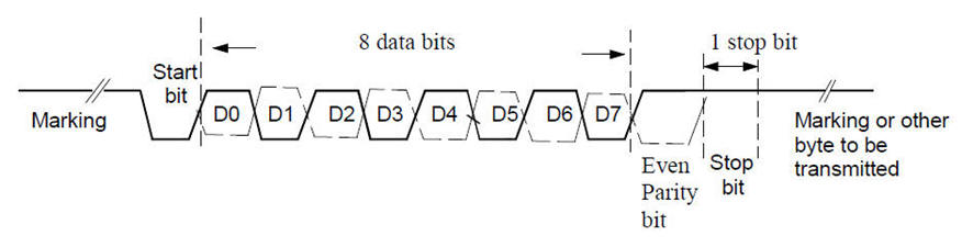
Let us design an USART. Fig. 1 shows the typical signal frame.
|
|
|
| Fig 1. Signal to transmit a byte of information. | |
Note: This project follows former CSD naming conventions and styles and is not updated.
This is a reference to read about these circuits.
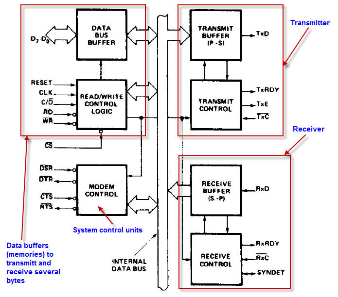
Example 1: Here you are an example classical chip from National Semiconductor, which was included in the firsts IBM PC in the eighties, the 8251A (or the INS8050), which is obsolete nowadays as a dual-in-line (DIL) chip component, due to the fact that its functionality is completely embedded in all microcontrollers, like in the PIC16F877A. We try to design here a simplified version of this chip.
|
|
|
| Fig 2. Classic USART chips. | |
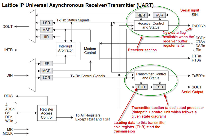
Example 2: Intellectual Property (IP) from Lattice Semiconductor on the reference design of a UART that can be synthesised in Lattice low-power and low-cost PLD. Note how a component like this one is professionally presented: Datasheet, VHDL and Verilog source files, testbench ("do" files), and an implementation guide to synthesise it all into a Lattice PLD using ispLEVER software (free and very similar to Altera's Quartus Prime or Xilinx Vivado). Open the datasheet and take a look at the transmitter and receivers' state diagrams.
|
|
|
| Fig 3. Lattice USART intelectual property. | |
Example 3: Intellectual Property (IP) from Intel also includes an UART that is compatible with the standard (and obsolete) chip 16550 UART from National Semiconductor (What Happened to National.com?). SC16C550B is another newer version from NXP. Companies like Eureka Technology or Digital Core Design designs specialised IP.
Thus, after studying this theory and commercial applications, let's draw our UART's block diagram.
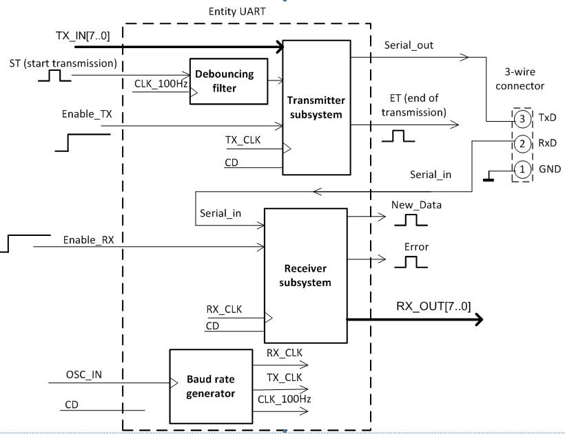 |
| Fig 4. Block diagram proposed for this project. |
2. Plan C2 based on a dedicated processor
The plan includes the problem division into several blocks, some of which were designed in previous exercises. Additionally, each cooperative group will be in charge of a different sub-module.
Block 1: Baud rate generator.
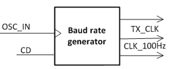 |
| Fig 5. Baud rate generator. |
Block 2: Transmitter datapath + Control Unit
Which resources are included in the transmitter datapath?
How does ths control unit work? Can you draw its stte diagram?
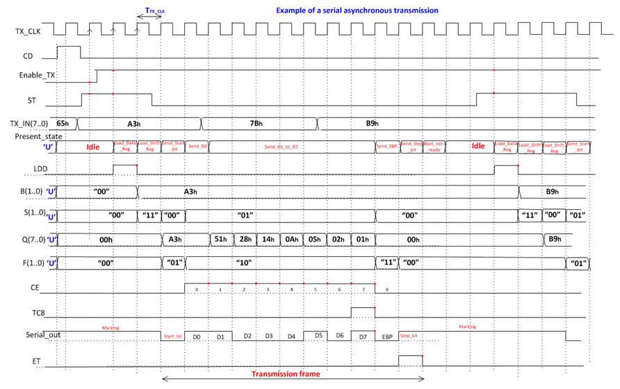
Here you are a file containing some sketches on the transmitter dedicated processor architecture. An example timing diagram (Visio).
|
|
| Fig 5. Transmitter signals. |
Block 3: Receiver datapath + control Unit
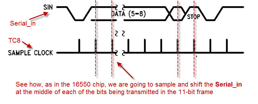
Here you are a file containing some sketches on the receiver dedicated processor architecture.
|
|
| Fig 5. Receiver signals. |
Block 4: Debouncing filter to generate "clean" and synhronosed digital pulses.
Analyse the tutorial in P6.
3. Development
There is a great deal of structural work here. Basically, a good strategy to finish the problem is the following:
-
Search and find all the basic components at the hierarchy levels 2 and 3. This components have had to be small projects in themselves, so that they work as expected.
-
Block I, II, III and IV have to be different projects. For example, all the 7 files for the Block I, the baud generator, become a project that can be tested autonomously in ModelSim. Also a Quartus Prime netlist viewer is recommended to visualise the structure synthisised by the EDA tool. Notice that sometimes it's better to finish the block before simulating. For instance, it is recommended to finish the transmitter unit (or the receiver unit) and then run a testbench to check it all, than simulate only the unit's datapath or control unit separately, because having to invent all the control and status signals between the control unit and the datapath is very time consuming.
Block 1: Baud rate generator. It works from the 50 MHz oscillator available in the DE0 board.
|
Chip 1: Baud_Rate_Generator All outputs are square waveforms (6 files) |
Chip 1: Freq_Div_326.vhd |
|
| Chip 2: Freq_Div_8.vhd | ||
| Chip3: Freq_Div_96.vhd | ||
| Chip 4: Freq_Div_100.vhd | ||
| Chip 2: T_flip_flop.vhd |
Block 2: Transmitter datapath + Control Unit
Synthesise the project for an Intel chip and verify it in the laboratory. There are several options in order to perform a demonstration:
-
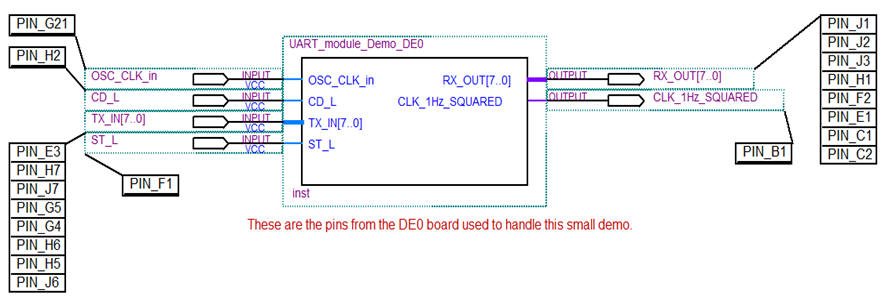
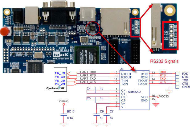
On a single board and using a loop defined on the top unit under test like shown in the previous picture. You may also automatically annotate the pin assignment, as shown in the following picture:
|
|
| Fig 5. Top module pin assignment connections. |
-
On a single board and using an external wire to make the loop.
-
Using two boards and interfacing them using a 3-wire cable.
-
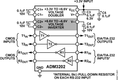
Using a board and a computer running a kind of HyperTerminal (for instance Tera Term) For example, the DE0 board, has the Analog Devices ADM3202 transceiver and the RXD and TXD signals are routed to pins U22 and U21 respectively. A 3-wire cable can be connected to the lateral 5-pin connector as shown in the picture bellow.
|
|
| Fig 5. ADM3202. |

|
 |
| Fig 5. ADM3202 to adapt voltage levels to RS232 standard. |
Block 3: Receiver datapath + control Unit
Block 4: Debouncing filter to generate "clean" and synhronosed digital pulses. Analyse the tutorial in P6.
| Number of VHDL files involved | Top block to be designed |
| 1 | Debouncing_filter.vhd |
Do file to simulate pulses for the debouncing filter. Debouncing_filter_functional_ModelSim.zip
UART Module top design (individual VHDL source files on the above table). Below other similar projects:
UART_module_Demo_DE0_finished.zip
| Number of VHDL files involved | Top block to be designed | Components (hierarchy level 1) | Components (hierarchy level 2) | Components (hierarchy level 3) |
| 22
(some components are used in more than one entity) |
UART_module.vhd | Block I Chip 1: Baud_Rate_Generator All outputs are square waveforms (6 files) |
Chip 1: Freq_Div_326.vhd |
|
| Chip 2: Freq_Div_8.vhd | ||||
| Chip3: Freq_Div_96.vhd | ||||
| Chip 4: Freq_Div_100.vhd | ||||
| Chip 2: T_flip_flop.vhd | ||||
| Block II Chip 2: Transmitter_unit.vhd (8 files) |
Chip 1: Transmitter_datapath.vhd | data_register_8bits.vhd | ||
| shift_register_10bit.vhd | ||||
| mux4.vhd | ||||
| parity_generator_8bit.vhd | ||||
| counter_mod8.vhd | ||||
| Chip 2: Transmitter_control_unit.vhd | ||||
| Block III Chip 3: Receiver_unit.vhd (9 files) |
Chip 1: Receiver_datapath.vhd | Chip 1: data_register_8bits.vhd | ||
| Chip 2: shift_register_10bit.vhd | ||||
| Chip 3: parity_checker_9bit.vhd | ||||
| Chip 4. counter_mod4.vhd | ||||
| Chip 5. counter_mod8.vhd | ||||
| Chip 6: counter_mod10.vhd | ||||
| Chip 2: Receiver_control_unit.vhd | ||||
| Block IV Chip 4. Debouncing_filter.vhd (1 file) |
4. Test (functional)
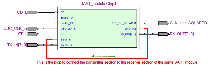
Once all the four blocks are finished and tested, integrate them all into the top UART (UART_module). And, once done, test it first using ModelSim. The following picture shows a demonstration where the transmitter is looped to the receiver, so that the TX_IN vector must appear at the RX_OUT once the transmission finished.
|
|
| Fig 5. Loop to simplify the test. |
5. Test (gate-level)
6. Prototyping
7. Report
| Home Term 24/25-Q1 Contact Products Electronic devices and companies Software Books Magazines Instruments DEE Library EETAC DEEL |

|
|
| Web activa des de 09/2001, @ F. J. Robert, J. Jordana. Web editat amb Microsoft Expression Web 4. El contingut és un complement als materials d'estudi del curs Circuits i Sistemes Digitals disponibles al campus digital Atenea. Llicència:Reconeixement 4.0 Internacional de Creative Commons |