|
|
|||||
Chapter 1 problems |
- D1.15 - |
3-digit code converter from BCD to binary radix-2 |
|||
|
|
|||||
1. Specifications
Large code converters such as a 3-digit BCD to binary radix-2 (BCD_bin_3digit) can be implemented using hierarchical schematics extracted and adapted from the 74184/74185 datasheet. This is applying plan C2.
The same project B3.15 is proposed in Chapter 3 for learning the basics of μC software organisation and basic digital I/O.
 |
|
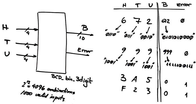
Fig. 1. BCD_bin_3digit symbol and truth table. H (hundreds digit), T (tens digit), U (units digit). |
PLA3 specifications include: symbol, truth table, data range, example commercial chips with similar functionality, etc. You may like to add theory to better explain and comprehend these circuits.
The Error signal may be implemented later, as a second design phase when the converter works. If you have time. What circuits may include? Any BCD number in H, T or U greater than 9 will generate an error flag.
Draw the testbench fixture and an example of timing diagram to be used later as stimulus in the VHDL verification of the synthesised circuit. Consider Min_Pulse = 14.3 ms. You can use as example test vectors for the BCD operand HTU one of the following options (add more numbers if you like):
-
Option #1: 772, 530, 680, 999, 032, 000, 228, 599
-
Option #2: 613, 013, 000, 125, 999, 321, 334, 100
-
Option #3: 201, 124, 999, 000, 808, 033, 761, 911
If we liked to test all the circuit, how long would it take to run the full verification?
CPLD or FPGA target chip options:
Target option #1.: MAX II
Target option #2.: Cyclone IV
MAX10 chips are not used because Intel Quartus does not generate the "*.sdo" file for running gate-level simulations.
Additional specifications for PLA4_1 for performing timing measurements and simulations:
Calculate the propagation delay in a given signal transition using gate-level simulations in VHDL.
Calculate the circuit's longest propagation delay and maximum speed for a given target chip using the timing analyser tool.
Be aware that the location of this project enhanced with timing simulation and measurements (section 5) is:
C:\CSD\P4\BCD_bin_3digit\files)
2. Planning
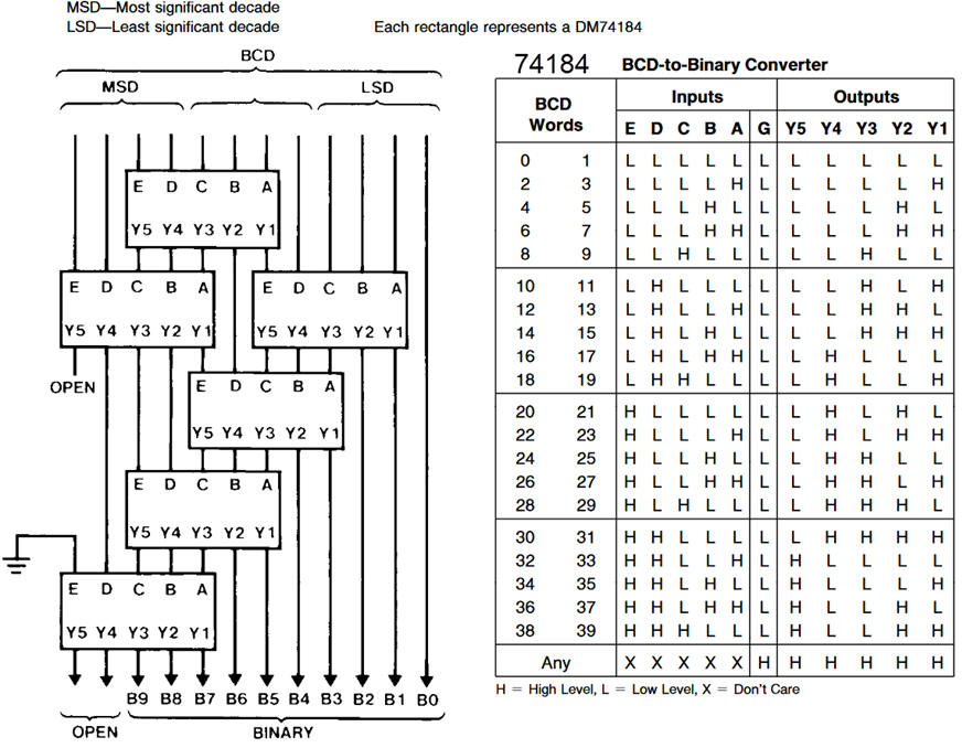
Studying the 74184 datasheet we see, as pasted in Fig 2, that the basic expandable component is cgoing to be the DM74184 chip that we can translate to VHDL. You can also analyse similar circuit from our product list. For example, in this tutorial DM74185 you can see the dual idea: from binary radix-2 to BCD. For example, in this tutorial project we designed the BCD_bin_mod40 component. The dual circuit from the same datasheet is the Bin_BCD_9bit.
 |
|
Fig. 2. Ideas and designs from datasheets. |
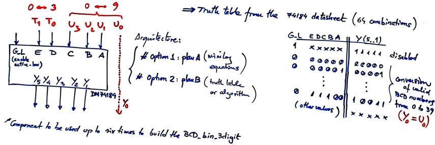
As a first step, you can redraw and adapt these schematics from the datasheet to our CSD conventions as shown in our other similar products. And, as a second step you can design the component DM184 using one of the options below.
 |
|
Fig. 3. Symbol and truth table for the DM74184 component.Its architecture can be obtained using plan A or plan B. |
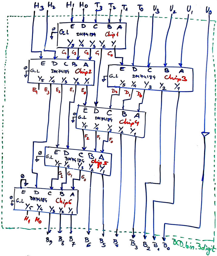
Hence, using this component DM74184, we can adapt and fuly annotate Fig. 2 as in Fig. 4.
 |
|
Fig. 4. Your plan for the BCD_bin_3digit ready for VHDL translation. |
Project location:
C:\CSD\P3\BCD_bin_3digit\(files)
DM74184 component options:
Option #1.: plan A
 |
|
Fig. 5a. Your plan for the DM74184 using plan A. Probably you will deduce the equations using the minimser app minilog. |
Option #2.: plan B
 |
|
Fig. 5b. Your plan for the DM74184 using plan B. Ypu can study how a similar circuit whas solved for the DM74185. and adapt it to the component in Fig. 3. |


