|
|
|||
|
|
Design Circuit_K using plan C2 |
Circuit_K plan A |
Circuit_K plan B |
|
|
|||
| MoD | MoM with MUX_4 | MoM with MUX_2 |
| 1. Specifications | Planning | Developing | Testing | Report | Prototype |
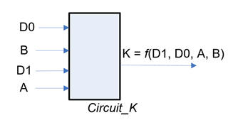
Implement the truth table written in Fig. 1 using a plan C2 architecture based on the method of decoders (MoD) proposed in L3.3.
  |
|
Fig. 1. Circuit_K to desing. K = f(D1, D0, A, B) |
| Specifications | 2. Planning | Developing | Testing | Report | Prototype |
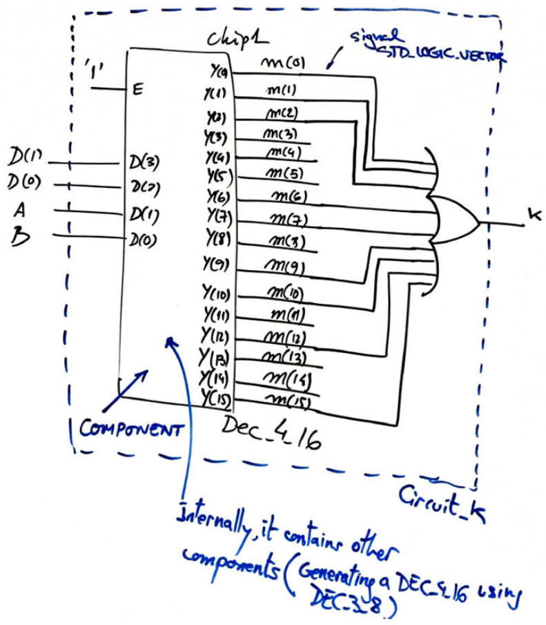
Fig. 2 shows how to invent the internal architecture based on MoD. Four inputs means using a Dec_4_16 component.
 |
|
Fig. 2. Circuit_K schematic using MoD. |
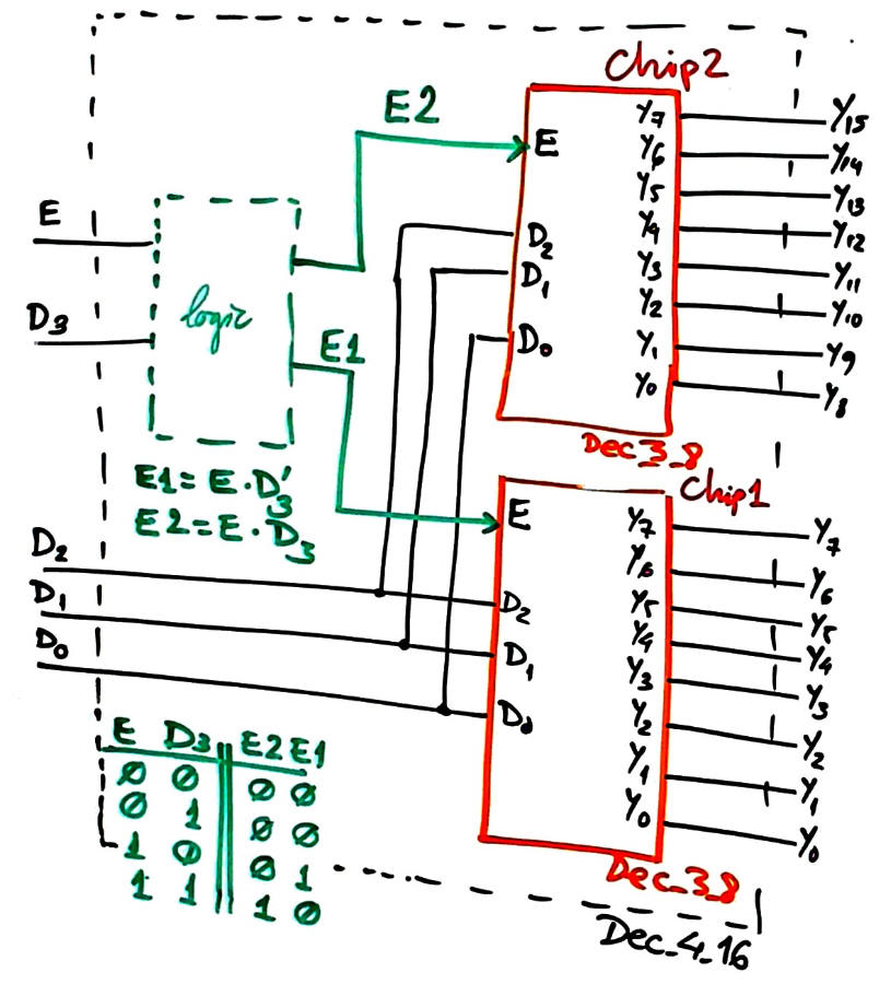
As an example on how many options are available for building blocks, Fig. 3 shows how to build the Dec_4_16 using components Dec_3_8, therefore applying plan C2 expandability. Chips Dec_3_8 at the same time can be composed of smaller blocs of the same kind such Dec_1_2, or instead be build using single-file plan A (equations) or plan B (flowchart). As shown in the truth table, extra logic is required to enable only one internal Dec_3_8 at a time, or disable both of them when E = '0'.
 |
|
Fig. 3. Circuit expandability: building the Dec_4_16 using Dec_3_8. |
Let us imagine the component Dec_3_8 using plan B as shown in Fig. 4.
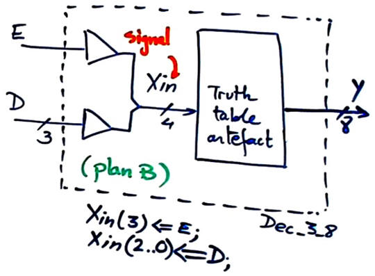 |
Fig. 4. Creating Dec_3_8 using plan B. |
In this way, this project will require three VHDL files: Circuit_K.vhd, Dec_4_16.vhd and Dec_3_8.vhd.
Testing the circuit will require the same testbench schematic Circuit_K_tb.vhd.
The project location may be:
C:\CSD\P3\Circuit_K\MoD\(files)
| Specifications | Planning | 3. Developing | Testing | Report | Prototype |
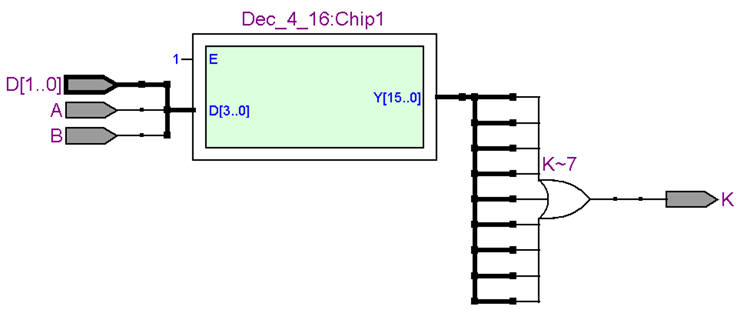
Translating the schematic into VHDL generates the following files: Circuit_K.vhd, Dec_4_16.vhd, Dec_3_8.vhd.
 |
|
Fig. 5. Circuit_K RTL view. |
| Specifications | Planning | Developing | 4. Testing | Report | Prototype |
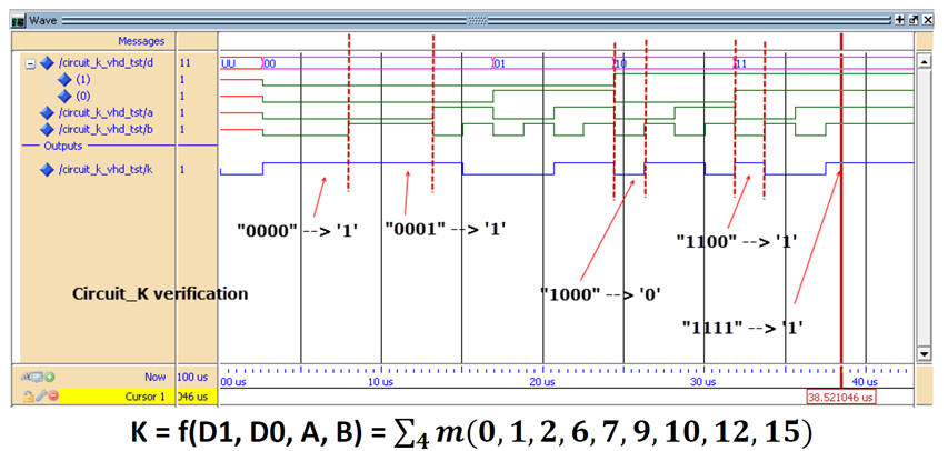
Using the same testbech from P1 Circuit_K tutorial Circuit_K_tb.vhd, we can verify our complete hierarchical structure as shown in Fig. 6.
 |
|
Fig. 6. Circuit_K functional simulation and results. |
| Specifications | Planning | Developing | Testing | 5. Report | Prototype |
Follow this rubric for writing reports.
| Specifications | Planning | Developing | Testing | Report | 6. Prototype |
We can use the DE10-Lite board to implement this project, as shown in Lab 1.2 for the similar Circuit_W.
| MoD | MoM with MUX_4 | MoM with MUX_2 |
| 1. Specifications | Planning | Developing | Testing | Report | Prototype |
Implement the truth table written in Fig. 1 using a plan C2 architecture based on the method of multiplexers and a MUX_4 as proposed in L3.3.
  |
|
Fig. 1. Circuit_K to desing. K = f(D1, D0, A, B) |
| Specifications | 2. Planning | Developing | Testing | Report | Prototype |
The project location may be:
C:\CSD\P2\Circuit_K_MoM_MUX_4\(files)
| Specifications | Planning | 3. Developing | Testing | Report | Prototype |
| Specifications | Planning | Developing | 4. Testing | Report | Prototype |
| Specifications | Planning | Developing | Testing | 5. Report | Prototype |
Follow this rubric for writing reports.
| Specifications | Planning | Developing | Testing | Report | 6. Prototype |
We can use the DE10-Lite board to implement this project, as shown in Lab 1.2 for the similar Circuit_W.
| MoD | MoM with MUX_4 | MoM with MUX_2 |
| 1. Specifications | Planning | Developing | Testing | Report | Prototype |
Implement the truth table written in Fig. 1 using a plan C2 architecture based on the method of multiplexers and a MUX_4 as proposed in L3.3.
  |
|
Fig. 1. Circuit_K to desing. K = f(D1, D0, A, B) |
| Specifications | 2. Planning | Developing | Testing | Report | Prototype |
The project location may be:
C:\CSD\P2\Circuit_K_MoM_MUX_2\(files)
| Specifications | Planning | 3. Developing | Testing | Report | Prototype |
| Specifications | Planning | Developing | 4. Testing | Report | Prototype |
| Specifications | Planning | Developing | Testing | 5. Report | Prototype |
Follow this rubric for writing reports.
| Specifications | Planning | Developing | Testing | Report | 6. Prototype |
We can use the DE10-Lite board to implement this project, as shown in Lab 1.2 for the similar Circuit_W.


