|
|
|||
|
|
Design the Circuit_K using plan B |
Circuit_K plan A |
Circuit_K plan C2 |
| B1: schematic | B2: flowchart |
| 1. Specifications | Planning | Developing | Testing | Report | Prototype |
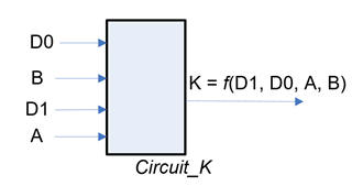
B1. Implement the truth table written in Fig. 1 using a behavioural plan B. based on capturing the truth table directly using a schematic interface.
  |
|
Fig. 1. Circuit_K to desing. K = f(D1, D0, A, B) |
| Specifications | 2. Planning | Developing | Testing | Report | Prototype |
The project location may be:
C:\CSD\P2\Circuit_K_B1\(files)
| Specifications | Planning | 3. Developing | Testing | Report | Prototype |
| Specifications | Planning | Developing | 4. Testing | Report | Prototype |
| Specifications | Planning | Developing | Testing | 5. Report | Prototype |
Follow this rubric for writing reports.
| Specifications | Planning | Developing | Testing | Report | 6. Prototype |
We can use the DE10-Lite board to implement this project, as shown in Lab 1.2 for the similar Circuit_W.
| B1: schematic | B2: flowchart |
| 1. Specifications | Planning | Developing | Testing | Report | Prototype |
B2. Implement the circuit in Fig. 1 using a behavioural plan B based on interpreting the truth table as a flowchart.
  |
|
Fig. 1. Circuit_K to desing. K = f(D1, D0, A, B) |
| Specifications | 2. Planning | Developing | Testing | Report | Prototype |
The project location may be:
C:\CSD\P2\Circuit_K_B2\(files)
| Specifications | Planning | 3. Developing | Testing | Report | Prototype |
| Specifications | Planning | Developing | 4. Testing | Report | Prototype |
| Specifications | Planning | Developing | Testing | 5. Report | Prototype |
Follow this rubric for writing reports.
| Specifications | Planning | Developing | Testing | Report | 6. Prototype |
We can use the DE10-Lite board to implement this project, as shown in Lab 1.2 for the similar Circuit_W.


