|
|
Bachelor's Degree in Telecommunications Systems and in Network Engineering |
|
|
|
||
|
|
Adder_1bit: behavioural single-file VHDL plan B |
|
|
|
||
Behavioural design of a 1-bit full adder circuit (Plan B)
| 1. Specifications | Planning | Developing | Testing | Report | Prototype |
Design a 1-bit adder using a behavioural description.
 |
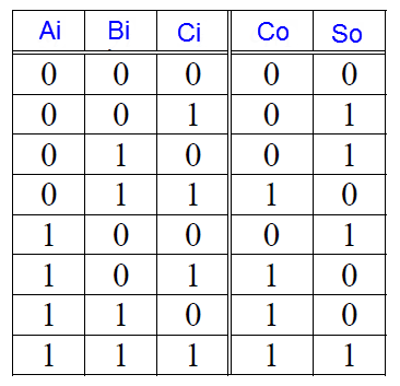 |
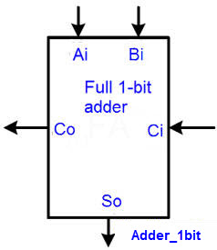
Fig. 1. Symbol and truth table of a 1-bit adder circuit. It is also called full adder. |
This in Fig. 2 is a simple sketch that represents the truth table in time. The idea of applying input vectors that can be any binary combination.
 |
|
Fig. 2. Timing diagram where all the inputs are applied sequentially and hence, the output is predicted accordingly to the truth table. |
| Specifications | 2. Planning | Developing | Testing | Report | Prototype |
The VHDL file will be named Adder_1bit.vhd, the same name given to the entity. The project name is Adder_1bit_prj.
Plan B) Behavioural (flat, single-file project). This Fig. 3 shows a plan to write the truth table immediately in VHDL.
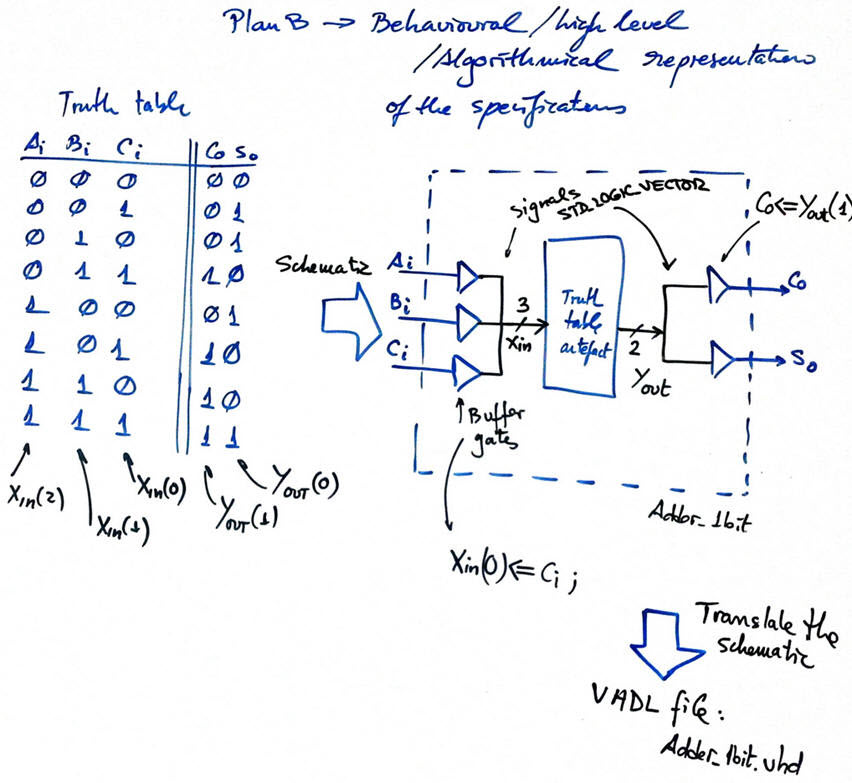 |
| Fig. 3. Schematic ready for translation to VHDL. The truth table is captured directly and the only additional resources required are some buffer gates to be able to use the entity names. |
The project location is C:\CSD\P3\Adder_1bit_B\(files)
| Specifications | Planning | 3. Developing | Testing | Report | Prototype |
Plan B behavioural. This is the translation to VHDL of the plan B1 above: Adder_1bit.vhd . Let us start a Quartus Prime project at the project location for a given target FPGA.
| Specifications | Planning | Developing | 4. Testing | Report | Prototype |
An example test bench Adder_1bit_tb.vhd. Run the VHDL simulation EDA tool to obtain and discuss the timing diagram. Remember that from the testing point of view, even if you have designed the Adder_1bit architecture using other plans, you can use all the time the same testbench file concerning the entity under test.
Draw the testbench fixture schematic ready for VHDL translation.
 |
Fig. 4. Test bench fixture to apply stimulus sto the circuit under test. |
The expected results for some operations are shown in Fig. 5.
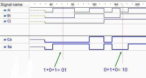 |
Fig. 5. Example testbench showing results |
| Specifications | Planning | Developing | Testing | 5. Report | Prototype |
Follow this rubric for writing reports.
| Specifications | Planning | Developing | Testing | Report | 6. Prototype |
We can use the DE10-Lite board to implement this project, as shown in Lab 1.2. Study the user manual and generate an Adder_1bit_top schematic to assign input and output pins. Another prototype concerning arithmetic operations is presented in Lab 4.
| Home Term 24/25-Q1 Contact Products Electronic devices and companies Software Books Magazines Instruments DEE Library EETAC DEEL |

|
|
| Web activa des de 09/2001, @ F. J. Robert, J. Jordana. Web editat amb Microsoft Expression Web 4. El contingut és un complement als materials d'estudi del curs Circuits i Sistemes Digitals disponibles al campus digital Atenea. Llicència:Reconeixement 4.0 Internacional de Creative Commons |