|
|
Bachelor's Degree in Telecommunications Systems and in Network Engineering |
|
| Analysis and design tutorials | Analysis and design assignments | Prototypes | Exam 1 | Exam 2 | Questions and assessment |
CSD EXA2: final exam examples and solution ideas |
1718Q1
Problem 1
Design a synchronous 5-bit one-hot code rotator (rotator_one_hot_5bit) with CE and reversibility (UD_L) using a FSM strategy. The output codes generated must be: "00001", "00010", "00100", "01000", "10000", "00001", …
a) Draw the symbol and name its inputs and outputs, Draw its function table. Sketch the state diagram and plot an example of a timing diagram.
b) Draw the FSM structure consisting of of CC1, CC2 and state register, indicating the name of the inputs and outputs. How many D_FF are necessary in this application if coding internal states in binary? How many D_FF are necessary if coding internal states in one-hot?
c) Draw the internal structure of the state register if the system is coded in one-hot.
d) Write the truth tables for CC1 and CC2.
e) Draw the flow chart for CC1 and its translation to VHDL code.
f) If the tCO (CLK to output propagation time) of a D_FF is 4.7 ns, and the propagation delay tP of a generic logic gate is 3.5 ns, estimate the maximum speed at which the rotator can work.
Some ideas on P1 solution.
Problem 2
Analyse the output waveforms and deduce the binary codes K[3..0] that generates the asynchronous circuit in Fig. 1 based on toggle flip-flops (T_FF).
 |
Fig. 1. Symbol and function table of a T_FF and the proposed example asynchronous circuit based on such T_FF. |
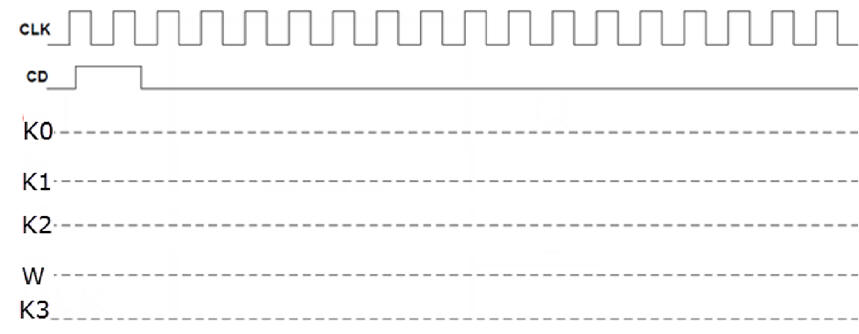 |
Fig. 2. Waveforms template. Indicate using dots which values are sampled and when. |
Some ideas on P2 solution.
Problem 3
We aim to implement a pulse-width modulation (PWM) generator that produces a 10 Hz fixed-frequency waveform with a duty cycle (DC = TON/TWAVE) that can be modulated form 0% to 100 %. See Fig. 3. The input will be the DC information encoded in 7-bit binary, so that DC = “0000000” represents the 0% modulation (all time ‘0’), and DC = “1100100” represents 100% (all time ‘1’). The start (ST) button toggles ON and OFF the output waveform Wave_out and the ON_LED.
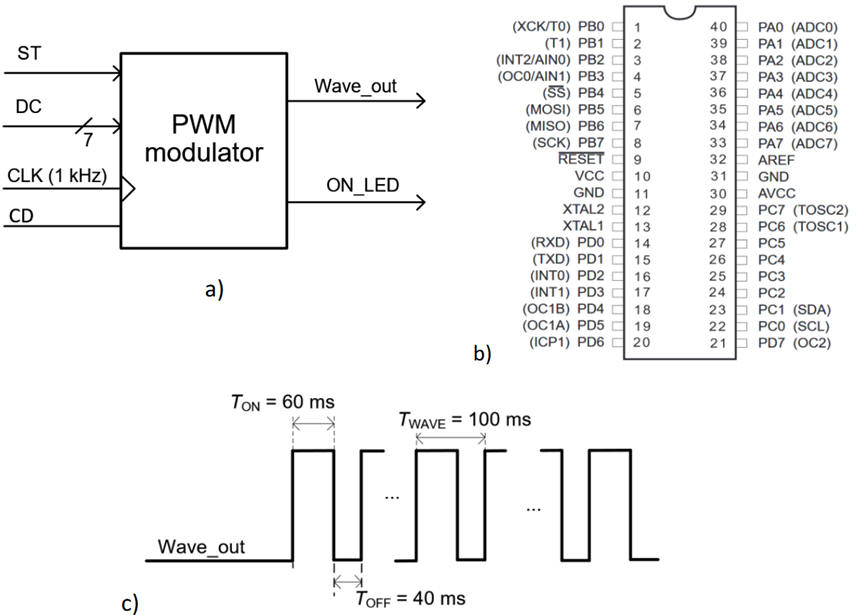 |
Fig. 3. a) Symbol of the circuit to be
designed. b) The ATmega8535 microcontroller. c) Example of a |
The general idea and the plan for the circuit may be to use a variable like Value_Q as a down counter that can be preloaded with the Value_Din = DC to count the TON time and then with the Value_Din = (100 – DC) to count the TOFF time. In this way a PWM waveform is generated accordingly to the parameter DC. For instance, if DC = 50% a square waveform will be generated. The CLK for this down counter may be the external 1 kHz signal by means of generating an interrupt every 1 ms.
1. Hardware. Draw the schematic showing where all the signals may be connected along with the reset and quartz crystal oscillator of 4 MHz to run this application using an Atmel ATmega8535 microcontroller chip.
2. Software. Represent a hardware-software diagram for the FSM indicating which inputs to read and write and which will interrupt, the name and bit organisation of the RAM variables, etc. Explain how the C code will be organised and the purpose of each function.
3. Draw a state diagram for the FSM indicating transitions and outputs, and name the states: Idle, Load_TON, DownCount_TON, Load_TOFF, DownCount_TOFF. Describe the tasks assigned to each state (output_logic), and how the system will evolve from one state to the next (state_logic).
4. Explain how to initialise some microcontroller pins to be digital inputs and some of them to be digital outputs (init_system).
5. Draw the flow charts and the equivalent C code for the functions read_inputs(), write_outputs() and ISR().
6. Draw the truth tables and their equivalent flow charts for the state_logic() and output_logic().
Some ideas on P3 solution.
| Home Term 26/27-Q1 Contact Products Electronic devices and companies Software Books Magazines Instruments DEE Library EETAC DEEL |

|
|
| Web activa des de 09/2001, @ F. J. Robert, Web editat amb Microsoft Expression Web 4. El contingut és un complement als materials d'estudi del curs Circuits i Sistemes Digitals disponibles al campus digital Atenea. Llicència:Reconeixement 4.0 Internacional de Creative Commons |