|
|
Bachelor's Degree in Telecommunications Systems and in Network Engineering |
|
| | ||
PLA9: On basic digital I/O. Designing a combinational circuit |
||
| NOTE:
This post lab assignment must be solved only after having completed
successfully lab session
Lab9 and
studied
P9 example because you
will copy and adapt materials from it. Study and use materials form lectures L9.1, L9.2, L9.3, L9.4. Microcontroller technology is different from Chaper 1 and Chapter 2 chips.New tools and concepts are required to adapt our applications. |
NOTE: EDA in use this semester: Proteus electrical simulator, Notepad++ editor (select C language), Microchip MPLABX and XC8 compiler.
Specifications
Use the options indicated by your instructor. The idea is to learn the basic of micocontrollers designing the same combinational circuit proposed in PLA2.
| Example of group assignments | |||
| Project number | Circuit entity | Pin option | |
| Group 1 | B3.10 4-bit radix-2 to Johnson code converter | Bin_Johnson_4bit | 1 |
| Group . 2 | B3.10 8-bit Johnson to binary radix-2 converter | Johnson_bin_8bit | 1 |
| Group 3 | B3.9 4-bit (byte) shifter operator | Shifter_4bit | 1 |
| Group . 4 | B3.7 2-digit multiplexed 7-segment display | Hex_7seg_MUX_2digit | 1 |
| Group . 5 | B3.10 4-bit radix-2 to Johnson code converter | Bin_Johnson_4bit | 2 |
| ··· | ··· | ··· | ... |
Study the project specifications in detail, use paper to discuss plans, connections, diagrams, RAM variables, etc. Solve in your computer tutorial projects first to learn the new tools. Do not invent C language instructions, but translate your schematics and flowcharts.
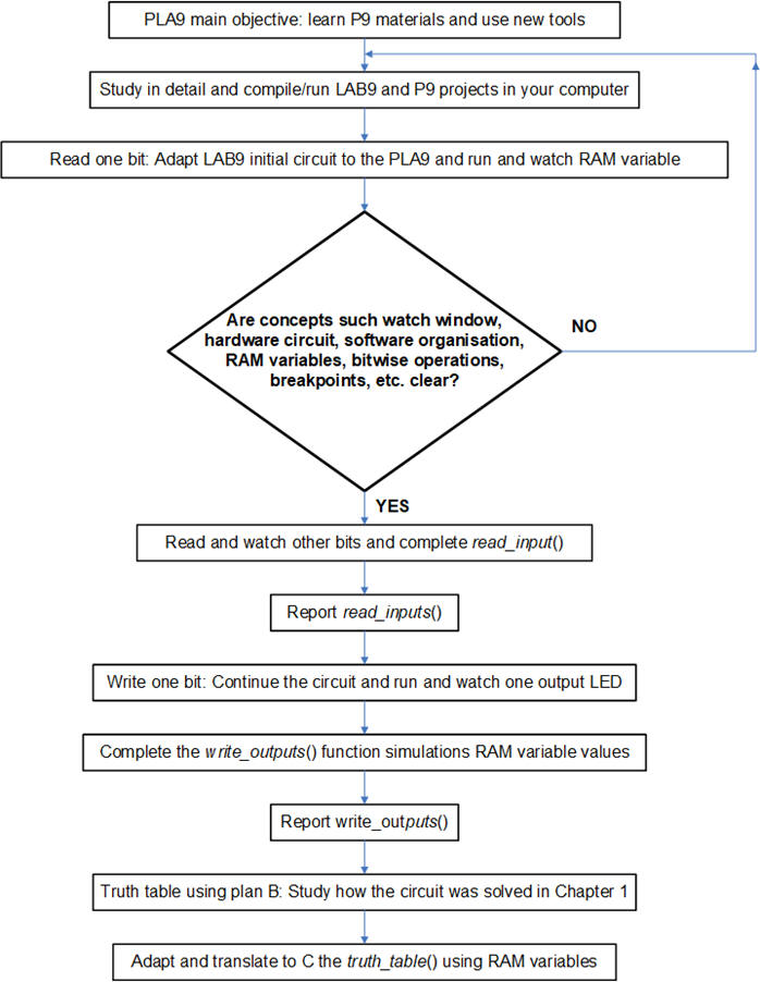
Keep in mind and run the following project flowchart for your step #1:
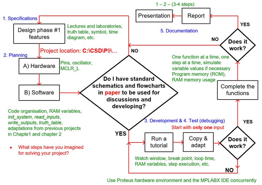
Some planning ideas to learn P9 basic I/O concepts and solving truth table algorithms inherited from Chapter 1 while solving PLA2 and PLA3 circuits. This is the initial hardware circuit and initial software source file to adapt to your PLA step by step. Use resistors, buttons, switches, LED, etc. Use your assigned project name and project folder to develop your circuits. Comment your C code while editing it.
Follow this rubric for writing reports.
| Home Term 24/25-Q1 Contact Products Electronic devices and companies Software Books Magazines Instruments DEE Library EETAC DEEL |

|
|
| Web activa des de 09/2001, @ F. J. Robert, J. Jordana. Web editat amb Microsoft Expression Web 4. El contingut és un complement als materials d'estudi del curs Circuits i Sistemes Digitals disponibles al campus digital Atenea. Llicència:Reconeixement 4.0 Internacional de Creative Commons |