|
Laboratory |
Laboratory 11: peripherals: [P11] LCD, [P12] TMR0 + dedicated processor Timer. Phase #1: time-base with external CLK phase #2: LCD phase #3 : internal TMR0 |
[19/12] |
|
This is the group post lab assignment PLA10_11 to be submitted at Atenea before the due date. Study and execute in your computer this LAB11 and the previous LAB10 tutorials before attempting to solve this post lab assignment. |
3.7.2. Examples: Timer
3.7.2.1. Timer (design phase#1)
This lab is for developing & testing a Timer circuit organised as in P8 (datapath & control unit). Timer's datapath is conceived as a RAM variable driven by an external CLK (50 Hz) signal connected to an external interrup (INT0). This external CLK is the time-base of the application defining a time resolution of 20 ms.
1. Specifications (Fixed-time timer. Phase #1: external CLK (INT1) time-base )
Design a fixed-time timer (for instance 18.5 s) as represented in Fig. 1. Dedicated processor (FSM + datapath), external INT
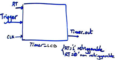 |
Fig. 1.Symbol. Interrupt-driven: Trigger signal a pushbutton connected at RB0/INT0. Interrupt-driven: CLK signal connected to RB1/INT1) to generate a time-base of 20 ms. |
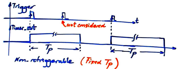
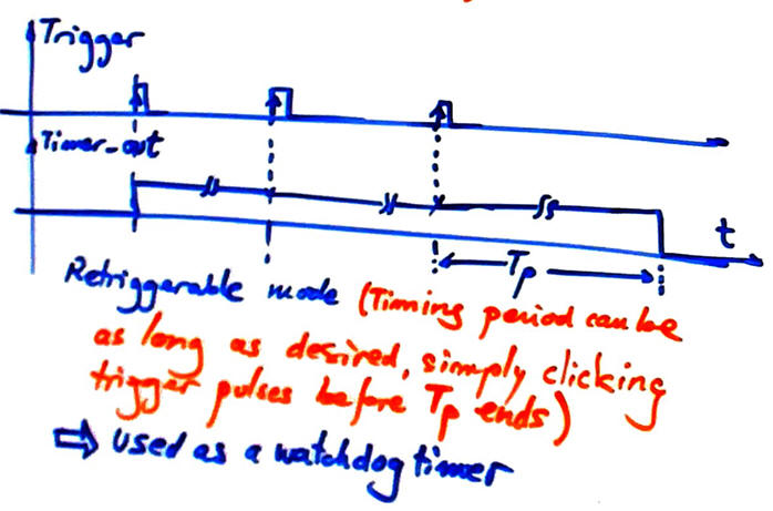
Two modes of operation: Retriggerable (RT=1) (see for example classic chip 74LS122/123) and non-retriggerable (RT=0) (see chip 74LS121). RT value by polling the switch at RA4 (level sensitive signal).
 |
|
Fig. 2. Basic waveform in non-retriggerable mode of operation. |
 |
|
Fig. 3. Basic waveform in retriggerable mode of operation. |
Other features: C language, coding in FSM style, dedicated processor approach, PICDEM2+ board. Compiler XC8, Microcontroller PIC18F4520.
2. Planning
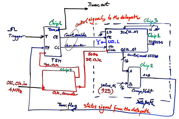
Study notes on how such (programmable) timer can be planned as in Chapter II using VHDL and FPGA/CPLD devices. In this way all the concepts involved will be known to you. Review as well P8 assignment on a programmable timer Timer_MMSS that is more complex but with the same organisation. Fig. 4 below shows yet another dedicated processor design. The FSM has to be able to attend trigger active edges to start operation and control the datapath, for instance an up binary counter.
 |
|
Fig. 4. Example dedicated processor to perform timer function. |
A) Planning hardware
Determine where to connect OSC, MCLR_L, Trigger, CLK, Timer_out and RT.
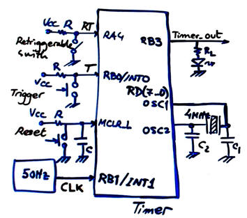 |
Fig. 5. Hardware connections. |
Step 2: Software. Draw the hardware-software diagram.
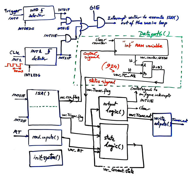 |
|
Fig. 6. Hardware-software diagram. |
B) Planning software
A FSM that also will include the datapath in its main loop.
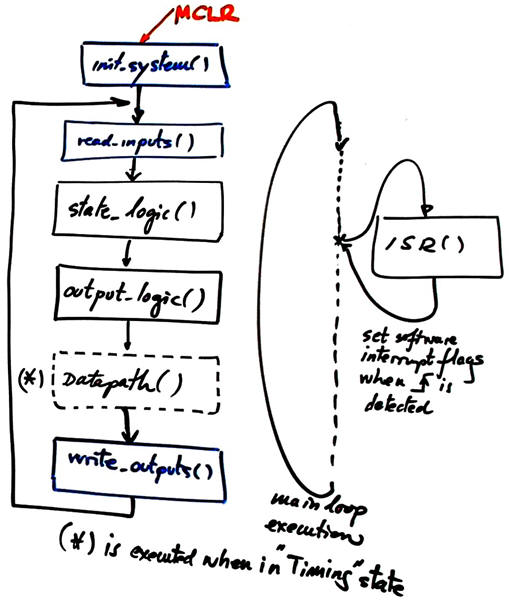 |
|
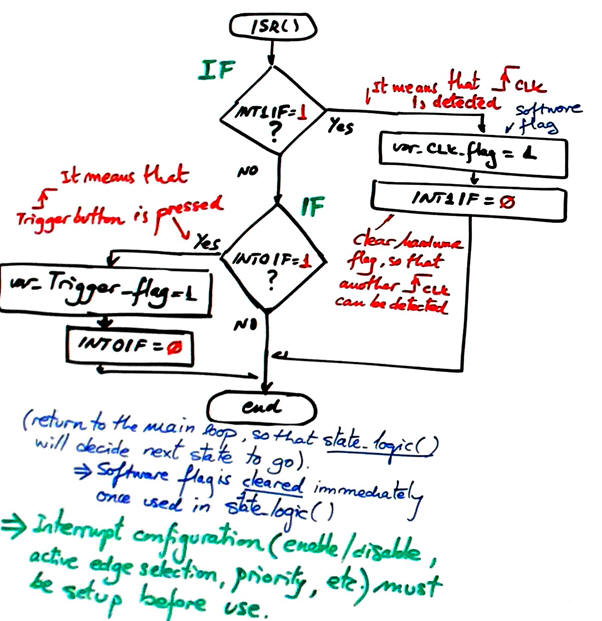
Fig. 7. General computer software organisation. ISR() will determine what is the interrupt source, trigger button or external CLK. Datapath function for counting CLK periods will be unused when IDLE. |
Draw the state diagram.
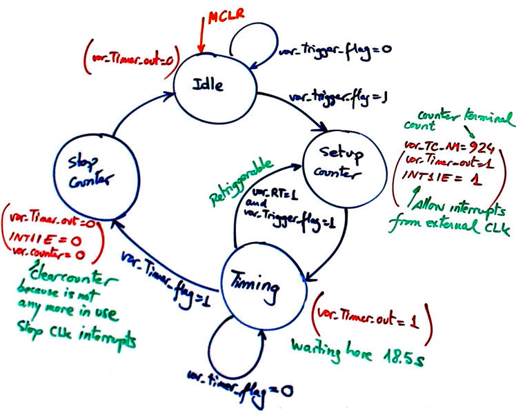 |
|
Fig. 8. State diagram for the FSM. The system is either idle or timing. However, peripherals and operating devices will require setting up and stopping extra states to prepare them to work properly. |
Program init_system() function, configuring ports and interrupts INT0 and INT1.
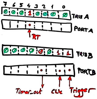 |
Fig. 9. Data direction registers (TRIS). PORTB pin 1 is INT1, PORTB pin 0 is INT0. PORTB pin3 is Timer_out. |
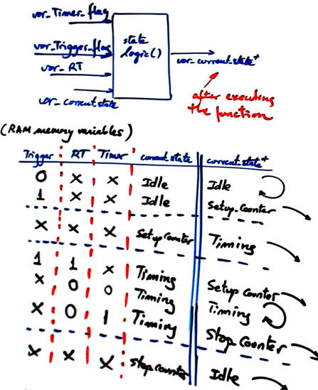
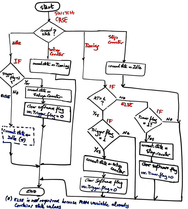
Program state_logic() so that all state transitions in Fig. 8 are implemented. Truth tables and flowcharts.
 |
|
Fig. 10. State logic and its equivalent behavioural flowchart (below) where C instructions are inferred with no difficulties. |
 |
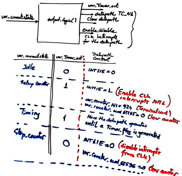
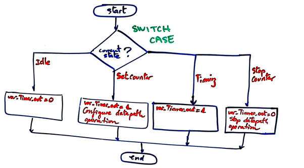
Program output_logic(). Truth tables and flowcharts. As seen in Fig. 6 hardware-software diagram, output logic has to generate Timer_out circuit's output and control signals for managing the datapath counter.
  |
|
Fig. 11. Output logic. Truth table and flowchart. |
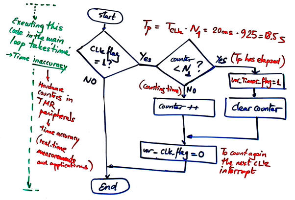
Program datapath() as a P7 counter solved now in software.
 |
|
Fig. 12. Datapath is a counter described using RAM variables. Be aware that executing assembly instructions requires some us, consequently introducing some systematic error if what we have in mind is measuring real-time. |
Write ISR() flowchart. so that the computer program can be sensitive to events such CLK rising edge and trigger button falling edges.
 |
|
Fig. 13. ISR() flowchart. |
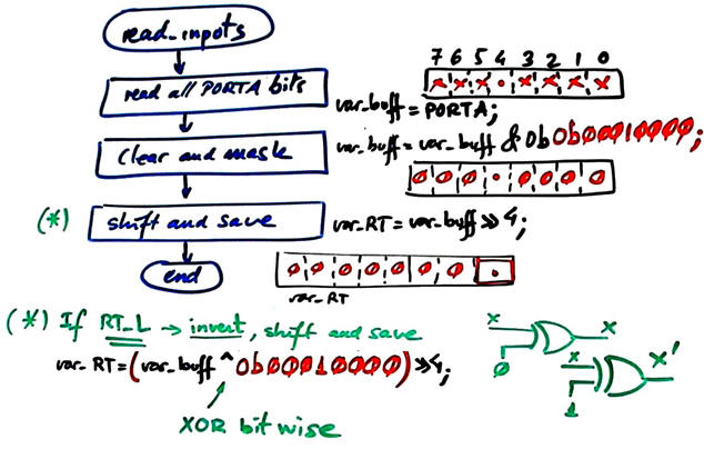
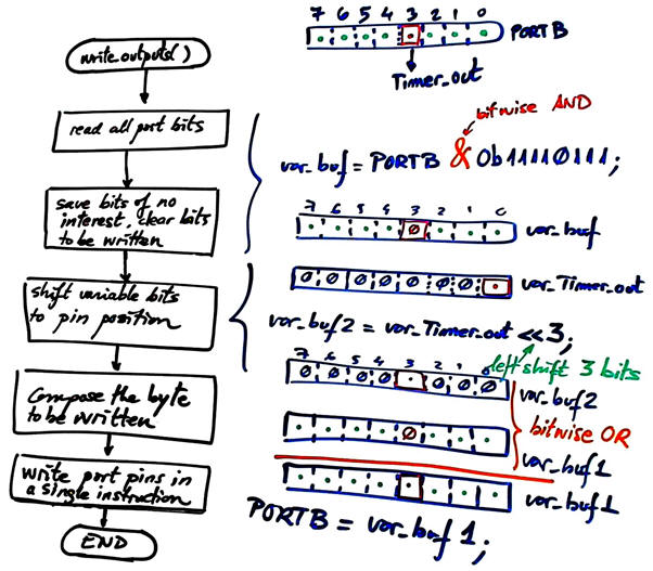
Program read_inputs(), write_outputs(). Truth tables and flowcharts.
 |
|
Fig. 14. Read_inputs() captures RT value when executed. This value is saved in a convenient RAM variable var_RT. |
 |
|
Fig. 15. Write_outputs() this time handles only var_Timer_out. |
Target chip PIC18F4520. Project location:
C:\CSD\P12\Timer\(files)
3. Developing and 4. Testing the design using EDA tools
A) Developing hardware
The basic timer represented in Fig. 16. Timer.pdsprj hardware.
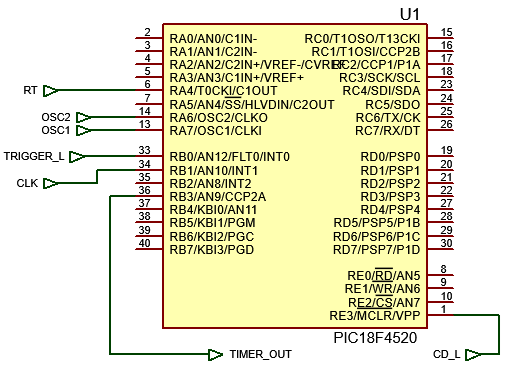 |
Fig. 16. Microcontroller connections. |
B) Developing software
Source file example Timer.c containing the translation of all planned flowchart .
C) Step-by-step testing
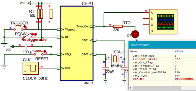
The idea is, as usual, write and run a bit of code with both windows, the hardware Proteus environment and the software IDE running simultaneously for easy debugging. Use watch window and break points to control the program sequence and monitor RAM variables of interest for each function.
 |
|
Fig. 17. Basic timer running while watching RAM variables. |
5. Report
Follow this rubric for writing reports.
6. Prototyping
Use the training boards and perform laboratory measurements to verify how the circuit works.
Modify timing period to 6.5 s. In this application the key point is the timing period precision. Is it 6.4998 s or 6.50001 s? How to measure timing precision? What can be done to improve it?
|
Laboratory |
Laboratory 11: peripherals: [P11] LCD, [P12] TMR0 + dedicated processor Timer. Phase #1: time-base with external CLK phase #2: LCD phase #3 : internal TMR0 |
[22/5] |
3.7.2.2. Timer_LCD (design phase#2)
Timer enhanced with LCD to show ASCII messages (and numerical data)on the LCD screen.
1. Specifications (Fixed-time timer. Phase #2: LCD peripheral)
Design a fixed-time timer (for instance 18.5 s) adding an LCD screen for representing information.
 |
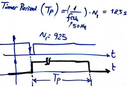 |
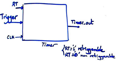
Fig. 1. The timer symbol and basic waveform in non-retriggerable mode of operation. |
|
Features:
- Same features as in design phase #1 Timer above.
- In a first step #1 information may be simply ASCII messages, in a second step #2, information may include dynamic data such time in seconds while down counting. The symbol is represented in Fig. 1.
2. Planning
A) Planning hardware
The LCD interface copying and adapting a previous example from P11.
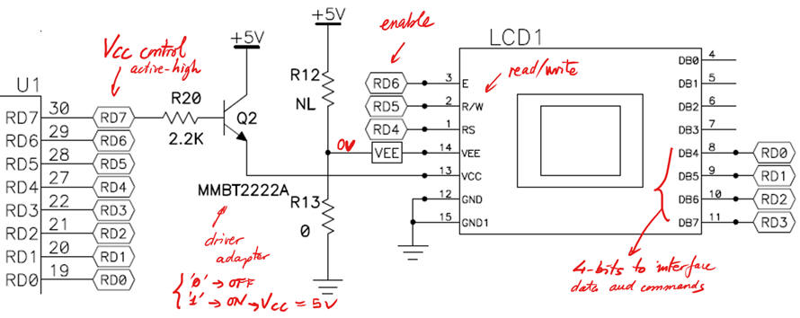 |
| Fig. 2. The LCD interface used in PICDEM 2 PLUS board can be replicated in Proteus. |
Electronic circuit.
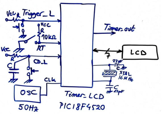 |
Fig. 3. Electronic circuit sketch. |
B) Planning software
Draw and discuss an state diagram and software organization. What states or signals have to be introduced to adapt the LCD? Hardware-software diagram
- Modify init_system() function.
- Modify state-logic() and output_logic(). Truth tables and flowcharts.
- Discuss read_inputs(), write_outputs() and ISR(). Truth tables and flowcharts.
Project location:
C:\CSD\P12\Timer_LCD\(files)
3. Developing the project using EDA tools
Study all the files in the basic Timer, design phase #1 above, this si the same application fully operational without LCD.
A) Developing hardware
Include LCD display. This is an example Timer_LCD.pdsprj harware.
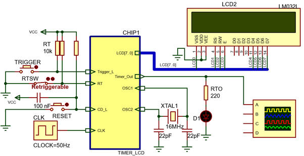 |
Fig. 4. Circuit captured in Proteus. |
B) Developing software
This is an example source file Timer_LCD.c to be compiled along with LCD libraries.
C) Step-by-step testing
Fig. 5 shows the circuit running representing ASCII characters on the LCD screen.
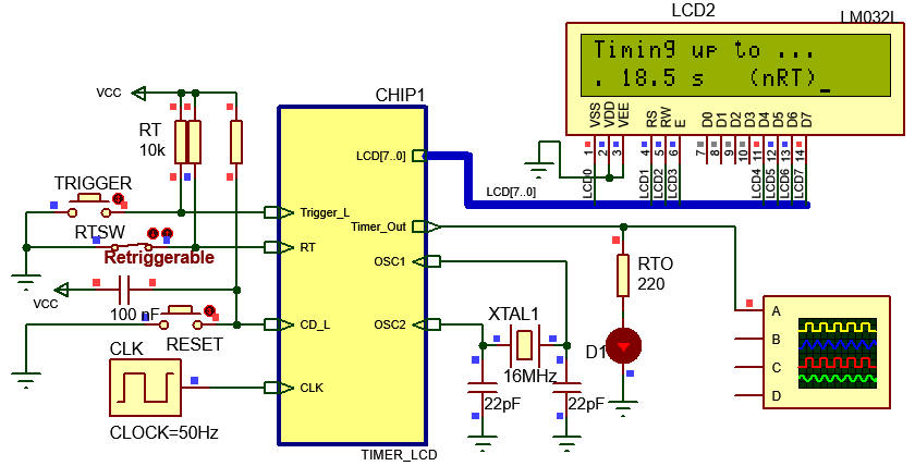 |
| Fig. 5. Timer with LCD running. |
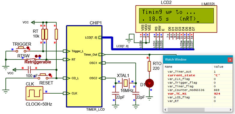
The idea is for easy debugging, write, compile and run a bit of code with both windows working interactevely: hardware Proteus environment and software IDE. Use the watch window and break points to stop and control the program sequence and monitor RAM variables of interest for each function.
 |
|
Fig. 3. The timer running while watching the main variables of the software. |
5. Report
Follow this rubric for writing reports.
6. Prototyping
This project may be uploaded to a PICDEM 2 PLUS board for laboratory experimetation.
Note on peripheral libraries. To solve projects involving specialised and complex peripherals you have to rely on external libraries, and there are a variety of them for the same purpose, depending as well on the C compiler. For instance, when installing the PLIBS for the XC8 compiler you can access to a variety of libraries including enhanced LCD functions (XLCD). Try this example circuit where all the required functions and header files from PLIBs are copied in the project folder allowing you to compile and run.
|
Laboratory |
Laboratory 11: peripherals: [P11] LCD, [P12] TMR0 + dedicated processor Timer. Phase #1: time-base with external CLK phase #2: LCD phase #3: internal TMR0 |
[22/5] |
3.8.3. Examples: Timer (continuation)
3.8.3.1. Timer_LCD_TMR0 (design phase#3)
Discuss how the functionality assigned to the counter and the time base circuits in the datapath can be covered by peripheral TMR0 embedded in the microcontroller. Replace the previous time-base (external CLK interrupt) by the peripheral TRM0.
- TMR0: hardware configuration bits and registers: CLK edge, CLK source, prescaler selection, TMR0 in 8-bit or 16 bit mode, hardware interrupt on overflow (terminal count) TMR0IF and variable var_TMR0_flag.
- Study the hardware-software diagram of the TMR0 timer/counter: prescaler (N1), counter TMR0 (N2), and (software) postscaler (N3) when required. How to increase counting capacity?
Questions:
- Measure simulator's "real-time" using break points and step mode.
- Watch variables of interest.
- Modify parameters to generate TP = 2.23 s.
- Modify parameters to generate TP = 5.00 s when XTAL OSC is 12 MHz.
1. Specifications for the fixed-time timer: design phase #3: TMR0 time-base
Design a fixed-time timer (for instance 18.5 s) as represented in Fig. 1 replacing the internal RAM variable acting as a datapath counter by TMR0 time-base of 1 us (FOSC = 4 MHz).
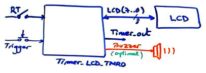 |
Fig. 1.Project entity is the same in phase #2 but supressing external CLK. |
Common features:
- The same as in project phase #1 Timer and phase #2 Timer_LCD .
- TMR0 peripheral to generate 1 μs time-base.
- Optional: Add a buzzer that will sound for 2 s at 1 kHz once the timing period has ended.
2. Planning
A) Planning hardware
Study how the TMR0 works, its configuration bits and interrupt mechanism. How to add a post-scaler to generate long counts?
If the optional buzzer is added it may wired at RC2 (as in PICDEM2plus board). The schematic is simpler from phase #2 because CLK is removed.
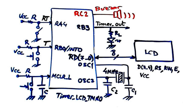 |
Fig. 2.Schematic. |
B) Planning software
Follow this adaptation. The datapath capable of counting real-time is TMR0 peripheral configured as a timer; the control unit is a FSM running in the main loop. Draw the hardware-software diagram as in Fig. 3 and the FSM state diagram (Fig. 4) to generate the output and to command the datapath.
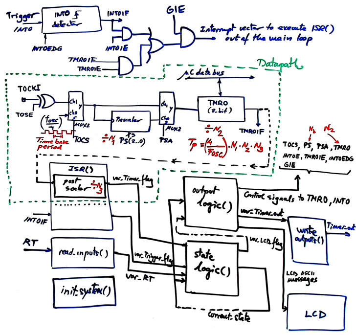 |
Fig. 3. Hardware-software diagram representing in dotted green lines the circuit that has become the datapath for calculating real-time from an internal time-base derived from system OSC. |
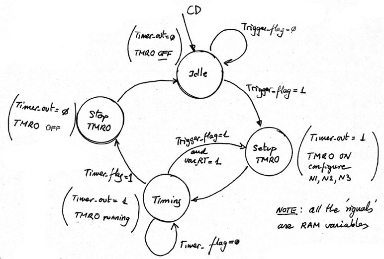 |
Fig. 4. State diagram for the FSM. |
Program init_system() function, configuring ports and interrupts and TMR0.
 |
Fig. 5. TRIS registers. |
Program state-logic() basically as in phase #2 or phase #1. Truth tables and flowcharts.
Program output_logic(). Truth table in Fig. 6.
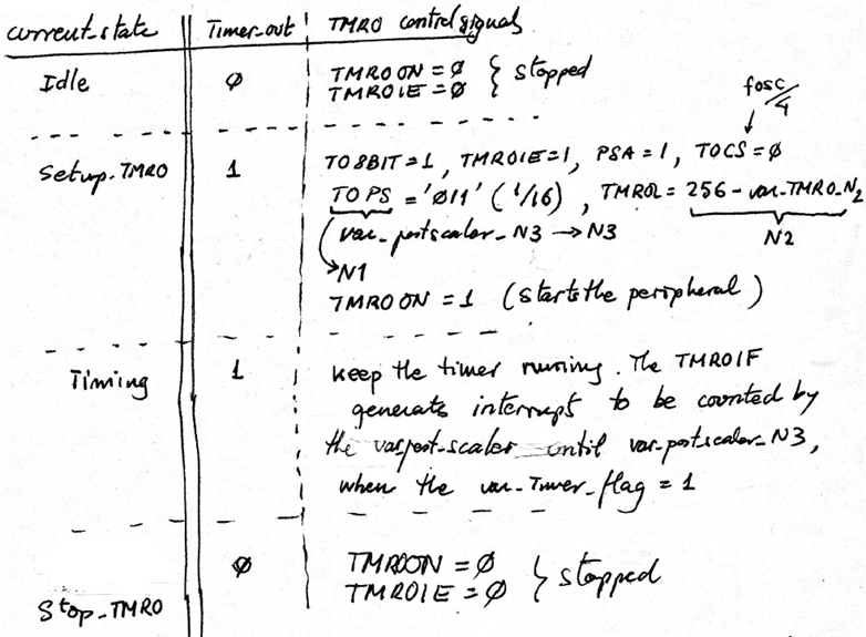 |
Fig. 6. Truth table for the output_logic() representing the instructions to the datapath and outputs. |
Program ISR() to acknowledge interrupts from TMR0 and INT0 solving as well the datapath operation of real-time counting.
 |
Fig. 7. ISR(). |
Program read_inputs(), write_outputs() as in phase #2 or phase #1.
Project location:
C:\CSD\P12\Timer_LCD_TMR0\(files)
3. Developing and 4. Testing using EDA tools
A) Developing hardware
This Timer_LCD_TMR0.pdsprj hardware including the LCD and the TMR0.
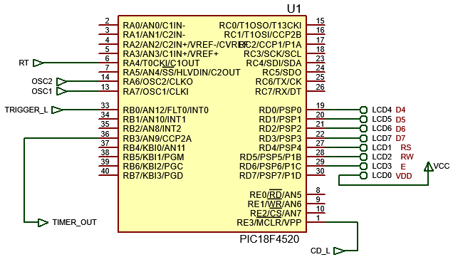 |
Fig. 8. var_Timer_flag is derived from internal TMR0. It means that another external for another purpose can be used in pin RB1/INT1. |
B) Developing software
This is the example software source code Timer_LCD_TMR0.c to be compiled along with LCD libraries.
C) Step-by-step testing
The idea is, as usual, write and run a bit of code with both windows, the hardware Proteus environment and the software IDE running simultaneously for easy debugging. Use the watch window and break points to control the program sequence and monitor RAM variables of interest for each function.
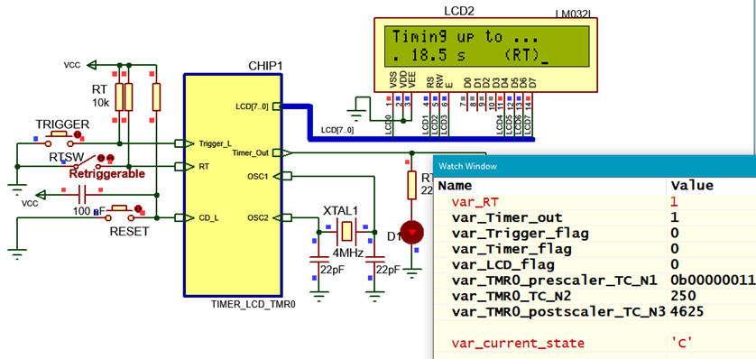 |
| Fig. 9. Circuit running and watching variables of interest. |
|
NOTE: A new feature: Fig. 10 is the same circuit Timer_LCD_TMR0.c to represent dynamic data while counting. Real-time processing is solved in Timing state. |
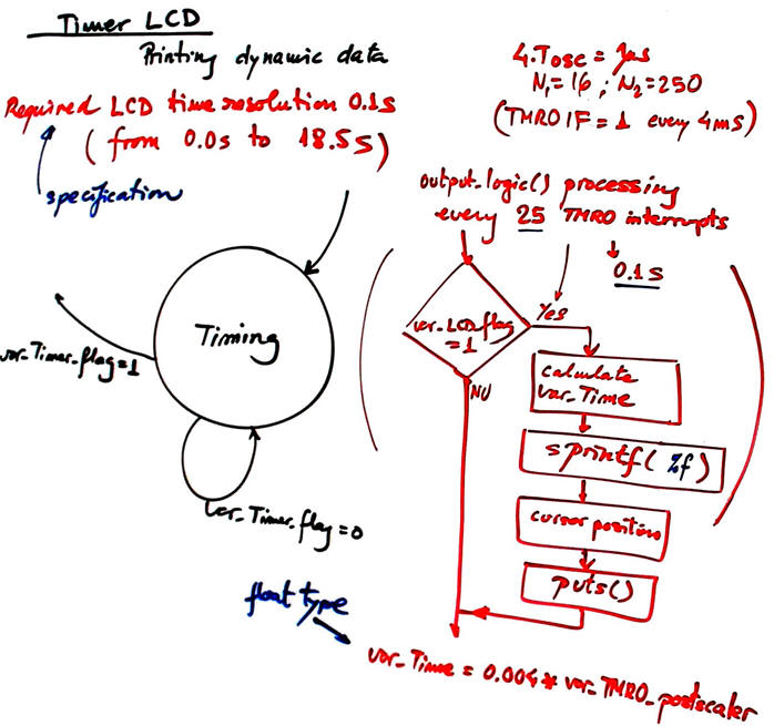 |
| Fig. 10. Displaying "real-time" in one-tenth of a second resolution on the LCD. |
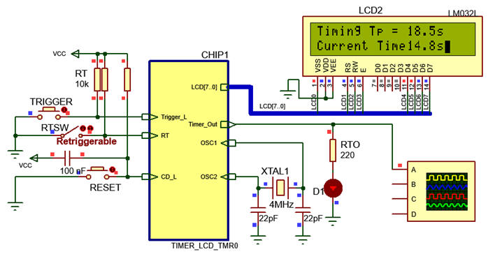 |
Fig. 11. Picture of the same timer representing and udating time every tenth of a second. |
5. Report
Follow this rubric for writing reports.
6. Prototyping
Use training boards and perform measurements to verify how the circuit works for real in laboratory.
In this application the key point is the precision of timing period. How to measure timer precision? What can be done to improve it?
How to represent as well a seconds count in the LCD?
Add the buzzer to sound the alarm when the timing period has finished. What king of modifications are required?
|
|
TMR2 can be used instead of TMR0 as proposed in this design phase #4: Timer_LCD_TMR2.
|
|
- PLA10_11 work in progress assessment


