|
|
|||||
Chapter 1 problems |
- D1.8 - |
5-bit Gray to binary and binary to Gray code converters |
|||
|
|
|||||
Project option #1: 5-bit Gray to binary converter Project option #2: 5-bit binary radix-2 to Gray converter
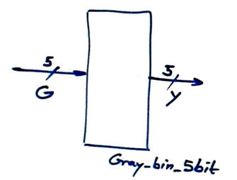
Design the 5-bit Gray to binary radix-2 code converter represented in Fig. 1.
The same project B3.8 is proposed in Chapter 3 for learning the basics of μC software organisation and basic digital I/O.
 |
Fig.1. Symbol of the Gray_bin_5bit converter. |
Draw an example of timing diagram to be used later as stimulus in the VHDL testbench when verifying the synthesised circuit. Consider Min_Pulse = 2.78 ms.
CPLD or FPGA target chip options:
Target option #1.: MAX II
Target option #2.: MAX 10
Target option #3.: Cyclone IV
2. Planning
Plan A structural circuit based on logic gates and equations in a single VHDL file. We have many estrategies, for instance:
option #1: use minilog to obtain PoS.
Project location:
C:\CSD\P2\Gray_bin_5bit_PoS\(files)
How many FPGA resources (logic cells, logic elements, etc.) are used? What is the percentage of the target chip used in this design?
option #2: use minilog to obtain SoP.
Project location:
C:\CSD\P2\Gray_bin_5bit_SoP\(files)
How many FPGA resources (logic cells, logic elements, etc.) are used? What is the percentage of the target chip used in this design?
Plan B behavioural approach writing the truth table or the high-level description or algorithm in VHDL in a single file (flat).
Project location:
C:\CSD\P2\Gray_bin_5bit_B\(files)
How many FPGA resources (logic cells, logic elements, etc.) are used? What is the percentage of the target chip used in this design?
After having studied P4 tutorials, additional questions can be added to our report. For instance:
-
Perform a gate-level simulation to measure propagation delays in a given signal transition.
-
Deduce the worst-case propagation delay running the timing analiser tool and calculate the circuit's maximum frequency of operation for the target chip used in the design.
Project option #2: 5-bit binary radix-2 to Gray code converter
1.- Specifications
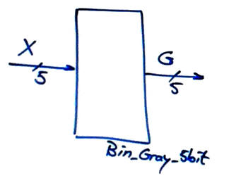
Design the 5-bit binary radix-2 to Gray code converter represented in Fig. 1.
 |
Fig.1. Symbol of the Bin_Gray_5bit converter. |
Draw an example of timing diagram to be used later as stimulus in the VHDL testbench when verifying the synthesised circuit. Consider Min_Pulse = 3.45 ms.
CPLD or FPGA target chip options:
Target option #1.: MAX II
Target option #2.: MAX 10
Target option #3.: Cyclone IV
2. Planning
Plan A structural circuit based on logic gates and equations in a single VHDL file. We have many estrategies, for instance:
option #1: use minilog to obtain PoS.
Project location:
C:\CSD\P2\Bin_Gray_5bit_PoS\(files)
How many FPGA resources (logic cells, logic elements, etc.) are used? What is the percentage of the target chip used in this design?
option #2: use minilog to obtain SoP.
Project location:
C:\CSD\P2\Bin_Gray_5bit_SoP\(files)
How many FPGA resources (logic cells, logic elements, etc.) are used? What is the percentage of the target chip used in this design?
Plan B behavioural approach writing the truth table or the high-level description or algorithm in VHDL in a single file (flat).
Project location:
C:\CSD\P2\Bin_Gray_5bit_B\(files)
How many FPGA resources (logic cells, logic elements, etc.) are used? What is the percentage of the target chip used in this design?
After having studied P4 tutorials, additional questions can be added to our report. For instance:
-
Perform a gate-level simulation to measure propagation delays in a given signal transition.
-
Deduce the worst-case propagation delay running the timing analiser tool and calculate the circuit's maximum frequency of operation for the target chip used in the design.
Project option #3: reversible 5-bit Gray/bianry and binary/Gray code converter
1.- Specifications
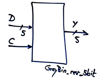
Design a reversible 5-bit code converter Gray/binary and binary/Gray using plan C2. Input C selects the code conversion direction: '0' ---> from Gray to binary; '1' ---> from binary to Gray.
 |
Fig.1. Symbol of the GrayBin_rev_5bit code converter. |
Draw an example of timing diagram to be used later as stimulus in the VHDL testbench when verifying the synthesised circuit. Consider Min_Pulse = 3.45 ms.
CPLD or FPGA target chip options:
Target option #1.: MAX II
Target option #2.: MAX 10
Target option #3.: Cyclone IV
2. Planning
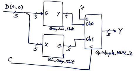
Fig. 2 shows an idea on how to connect components to generate such reversible product.
 |
Fig.2. Hierarchical architecture using components. |
How many FPGA resources (logic cells, logic elements, etc.) are used? What is the percentage of the target chip used in this design?


