|
|
Bachelor's Degree in Telecommunications Systems and in Network Engineering |
|
|
|
||
|
|
Int_Comp_8bit plan C2: hierarchical multiple-file VHDL |
|
|
|
||
1. Specifications
Two main objectives:
1) Invent a comparator for 8-bit signed integers Int_Comp_8bit as drawn in Fig. 1. Three outputs are required: GT (greater than) to detect when A > B, EQ (equal to) to detect when A = B, and LT (less than) to detect when A < B.
Design the Int_Comp_8bit using plan C2 and Comp_8bit components and logic gates, in the same way the Int_Add_Subt_8bit was designed using Adder_8bit and logic gates.
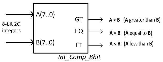 |
Fig. 1. a) Symbol of the project. Input operands A(7..0), B(7..0) are 8-bit integers expressed in 2C. What is the range the input data? |
 |
b) Draw the Int_Comp_8bit truth table. |
|
|
c) Sketch of a timing diagram showing how it performs several
integer operations. |
2) Calculate the circuit's maximum speed for a given target PLD chip.
Once the circuit works and is tested functionally as usual, perform a gate-level simulation to determine the circuit's propagation delay in a given transition and also circuit's maximum speed of operation using the timer analyser tool.
You can solve the project for two chips and compare results:
- Intel FPGA Cyclone IV EP4CE115F29C7N
- Intel CPLD MAX II EPM2210F324C3
2. Planning
The algorithm for comparing integer numbers in 2C has to be discussed. This is a ref. on building Int_comp_8bit.
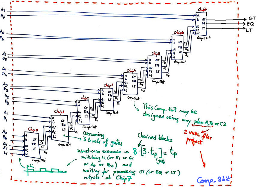
We have in mind to design a comparator for integer numbers using the radix-2 comparator and logic gates if necessary, in the same way that we designed the Int_Add_Subt_8bit using Adder_8bit and logic. Fig. 2 shows what happens when both, A and B are positive or negative.
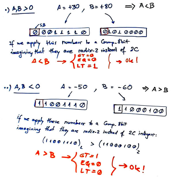 |
Fig. 2. Comparison of two positive integers or two negative integers. |
Fig. 3 shows the trick to be used when comparing positive and negative numbers, we can swap operands sign bits in order to use a conventional radix-2 Comp_8bit.
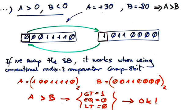  |
Fig. 3. Comparison of negative and positive integers. Thus, the algorithm is to swap sign bits. |
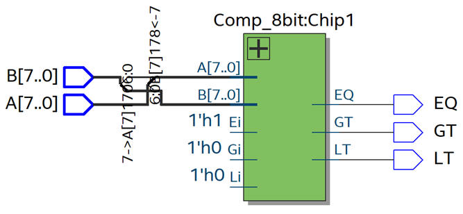
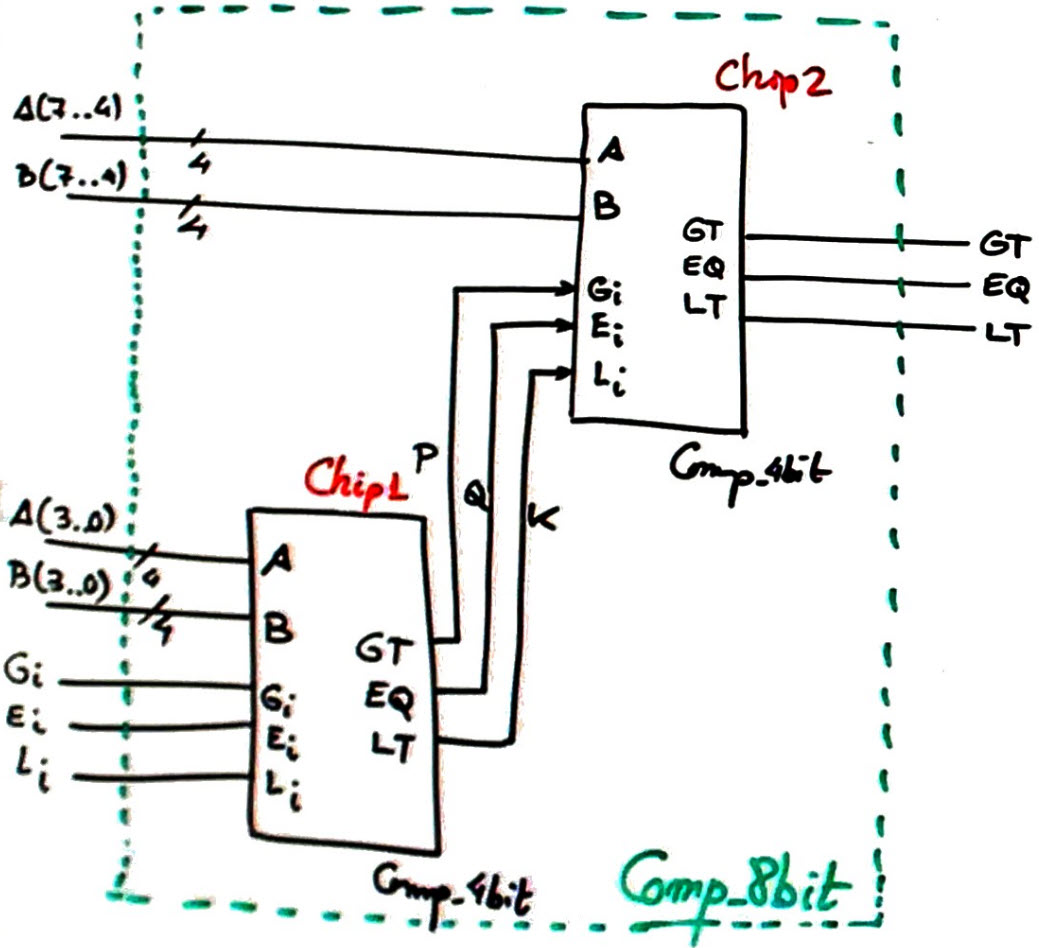
This time, no extra logic is required for the implmenttion in Fig. 4. Chip1 is a conventional radix-2 Comp_8bit.
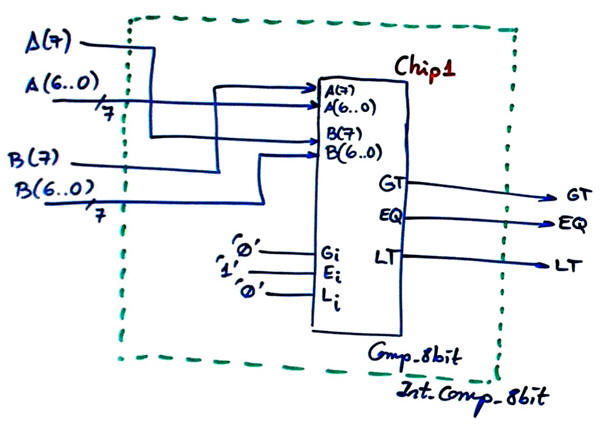 |
Fig. 4. Proposed plan C2 circuit. |
A radix-2 comparator Comp_8bit has to be designed previoulsy, for instance, adapting the schematic in this example project Comp_10bit to only 8 bits.
Alternatively, a radix-2 comparator Comp_8bit may be built chaining only two Comp_4bit plan A or Comp_4bit plan C2. So, several options are possible and in the end we will be able to compare solutions.
Project folder:
C:/CSD/P4/Int_Comp_8bit/(files)
Translate the circuit in Fig. 4 to VHDL as usual: Int_Comp_8bit.vhd.
Find Comp_8bit.vhd and the Comp_1bit from P3 tutorials on radix-2 arithmetic circuits.
Run the EDA tool to synthesise the circuit for a given FPGA target chip (for instance, MAX II CPLD EPM2210F324C3).
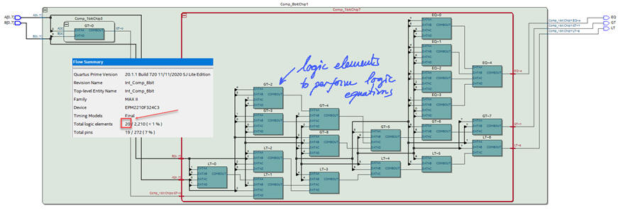
Print and comment the RTL schematic. Is it like what you had sketched in the plan?
|
|
| Fig. 5. RTL schematic. |
Synthesising this Int_Comp_8bit requires 20 logic elements in a MAX II CPLD device (Comp_1bit is solved using plan A).
|
|
| Fig. 6. Technology view. How many logic elements are used in this design? |
4. Testing (functional simulation)
The testbench fixture containing the main ideas and concepts involved in this schematic is represented in Fig. 7.
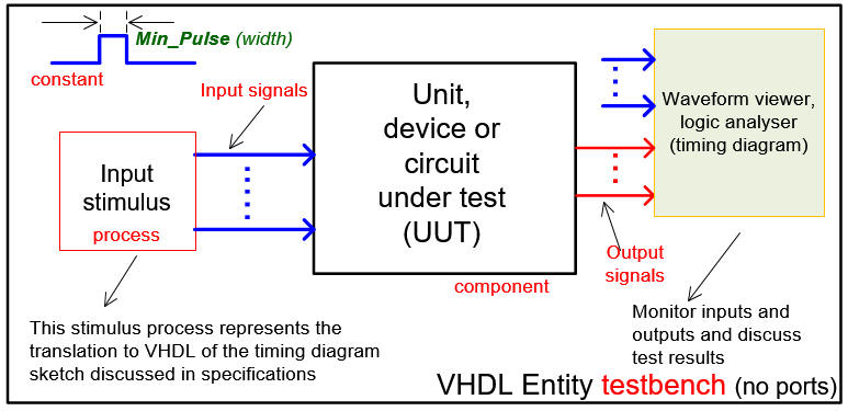 |
Fig. 7. Testbench VHDL schematic. |
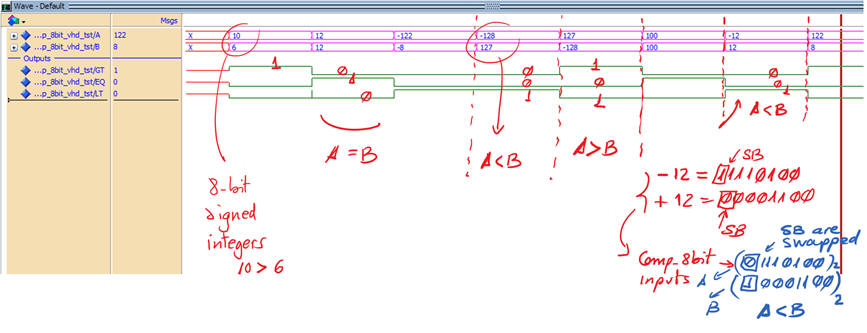
Convert the initial timing diagram sketch into a VHDL testbench like in this file Int_Comp_8bit_tb.vhd writing input activity process and Min_Pulse constant in the template produced by the EDA tool. Use positive and negative numbers as inputs to the circuit.
Run the EDA VHDL simulator and demonstrate how the circuit works adding comments to the printed sheet of paper containing the waveforms.
|
|
Fig. 8. Example test with some input vectors A, B. |
5. Testing (gate-level simulation)
VHDL design flow shows how gate-level simulations represent the 5th design step. The idea is to build a circuit prototype ready for laboratory experimentation and characterisation only when the circuit is fully tested.
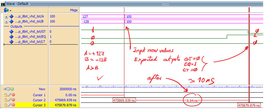
Run a gate-level simulation to measure the propagation delay in a given transition.
|
|
Fig. 9. Example waveform for the Int_Comp_8bit showing how a given input vector is computed over time generating wrong results until all signals have propagated through the circuit. In this transition it takes 10 ns to obtain the correct result. |
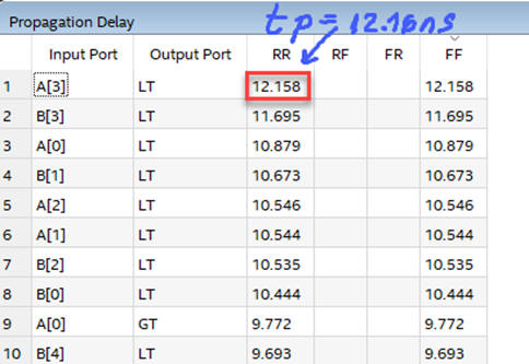
Use the timing analyser tool to determine worst-case scenario, and thus the maximum speed of comparison operations. In this example, the comparator can handle 82.2 millions of comparisons per second.
|
|
Fig. 10. Timing analyser spreadsheet. For a target chip MAX II the longest propagation time is tP = 12.16 ns. |
Repeat measurements for Intel Cyclone IV, and compare results.
Perform a simulation to show that the circuit cannot produce correct results when the Min_Pulse constant is less that the worst case delay.
6. Report
Follow this rubric for writing reports.
| Home Term 24/25-Q1 Contact Products Electronic devices and companies Software Books Magazines Instruments DEE Library EETAC DEEL |

|
|
| Web activa des de 09/2001, @ F. J. Robert, J. Jordana. Web editat amb Microsoft Expression Web 4. El contingut és un complement als materials d'estudi del curs Circuits i Sistemes Digitals disponibles al campus digital Atenea. Llicència:Reconeixement 4.0 Internacional de Creative Commons |