|
|
Bachelor's Degree in Telecommunications Systems and in Network Engineering |
|
|
|
||
|
|
Comp_10bit plan C2: structural hierarchical multiple-file VHDL |
|
|
|
||
Structural design of a 10-bit expandable comparator (Plan C2)
1. Specifications
Design a 10-bit expandable comparator Comb_10bit using hierarchical design based on components of the same kind, for instance Comp_1bit or Comp_4bit.
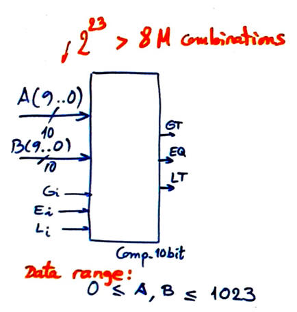
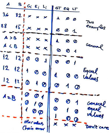
Comp_10bit has the symbol and truth table represented in Fig. 1.
|
|
| Fig. 1. Symbol and truth table of a 10-bit comparator with extra signals for expandability. |
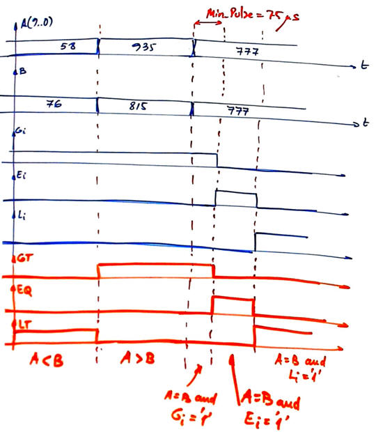 |
| Fig. 2. Example of timing diagram. Outputs are deduced from the circuit's truth table. |
2. Planning
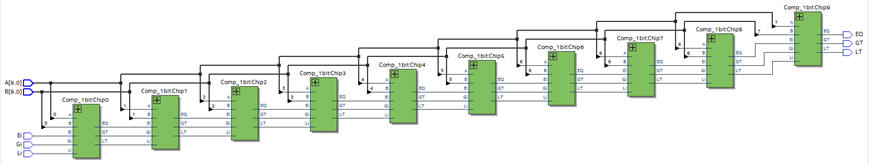
Plan C2. Structural hierarchical. This means a plan based on interconnecting or chaining components (circuit expansion) and extra logic when necessary. For instance, Fig. 3 is a plan using Comp_1bit components and signals.
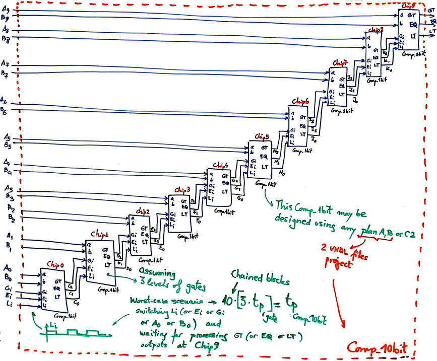 |
Fig. 3. Example plan of Comp_10bit partially annotated. You must draw and complete this schematic in a sheet of paper annotating all signals and chip references before VHDL translation. |
The VHDL top entity is named Comp_10bit.vhd and the project name is Comp_10bit_prj.
Project location:
C:\CSD\P3\Comp_10bit\(files...)
3. Developing the project using EDA tools
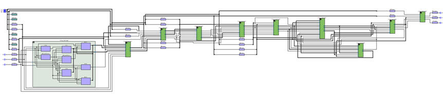
This is the 10-bit comparator Comp_10bit.vhd that corresponds exactly to the sketch in Fig. 3. Run a EDA project to synthesise the circuit. Fig. 4 shows an example of RTL schematic generated after the synthesis process.
 |
| Fig. 4. RTL view from Intel Quartus Prime. |
Get the component Comp_1bit that is used up to 10 times from tutorials plan A or plan B or plan C2. Anyone of them is perfectly valid. Note that if you like to use the Comp_1bit from plan C2, other components such MUX_2, MUX_4 and MUX_8 will become part of this project too, enlarging the hierarchy.
 |
| Fig. 5. Example technology view for a Cyclone IV FPGA chip. |
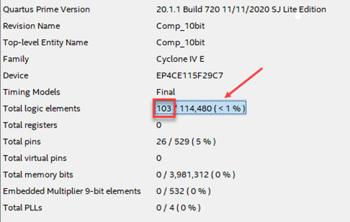
How many resources (logic elements) are used? It uses 103 logic elements.
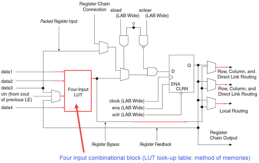 |
| Fig. 6. Cyclone IV logic cell architecture. Only the combinational section is used in Chapter 1 projects. EP4CE115F29C7 FPGA contains up to 114480 logic elements (LEs). |
4. Testing and validating the design
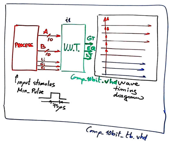
Test bench schematic for validating our design is always the same:
 |
|
Fig. 7. Testbench fixture. |
Fig. 2 timing diagram can be translated to a VHDL testbench process. An example test bench Comp_10bit_tb.vhd from where to copy and adapt vector stimulus input signals and constant Min_Pulse.
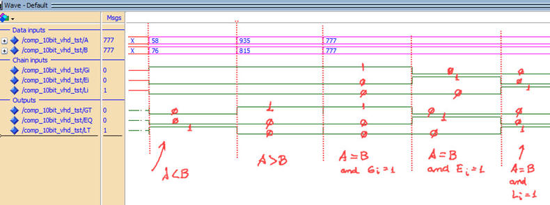
Run the VHDL simulation EDA tool to obtain and discuss the timing diagram.
 |
|
Fig. 8. Example testbench showing results. |
5. Testing at the gate-level the technology schematic to measure circuit's speed
Using a gete-level simulation is possible to measure propagation delays at a given signal transition. How long does it take to propagate signals from a given switching input to an output?
 |
|
Fig. 9. Example testbench showing results. |
Using the timer analyser tool is possible to measure the worst-case propagation time scenario, and thus determine the maximum circuit's speed for processing comparisons.
If Comp_10bit is invented using a tree architecture based on Comp_4bit as shown in 74LS85 datasheet, intead of a full chain of Comp_1bit blocks, circuit speed will be faster.
6. Report
At least five handwritten sheets of paper as usual in CSD. Follow this rubric for writing reports.
7. Prototyping
Use training boards and perform laboratory measurements to verify how the circuit works.
| Home Term 24/25-Q1 Contact Products Electronic devices and companies Software Books Magazines Instruments DEE Library EETAC DEEL |

|
|
| Web activa des de 09/2001, @ F. J. Robert, J. Jordana. Web editat amb Microsoft Expression Web 4. El contingut és un complement als materials d'estudi del curs Circuits i Sistemes Digitals disponibles al campus digital Atenea. Llicència:Reconeixement 4.0 Internacional de Creative Commons |