|
|
Bachelor's Degree in Telecommunications Systems and in Network Engineering |
|
|
|
||
|
|
MUX_8 plan B: Behavioural single-file VHDL (flat) |
|
|
|
||
1. Specifications
Design a MUX_8 in a programmable logic device (PLD) target chip with specifications similar to the classic 74HCT151 chip, following our plan B, and using our VHDL design flow and EDA tools for developing and testing.
The chip's logic family (technology), whichever it is TTL, LS, S, CMOS, AS, HC, HCT, F, etc. is not important because the circuit wil be targeted for a PLD from Intel, Xilinx or Lattice Semiconductor. Thus, only the chip's functionality is considered.
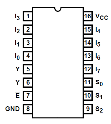 |
Fig. 1. Package and pin enumeration of classic 74HCT151 chip. We have to interpret and rename the pins because every company has its own way to name inputs/outputs and organise their product datasheet (Nexperia, Toshiba/Renesas, ON semiconductor, etc.); thus, in CSD we have decided to use our own naming style and rewrite the truth table accordingly. For instance, the pin 12 will be always our input Ch7, an so the same with all the other pins. |
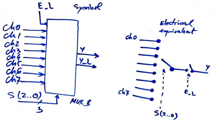
Examine Texas Instruments 74HCT151 datasheet and represent symbol and truth table, renaming inputs and outputs as shown in Fig. 2.
|
|
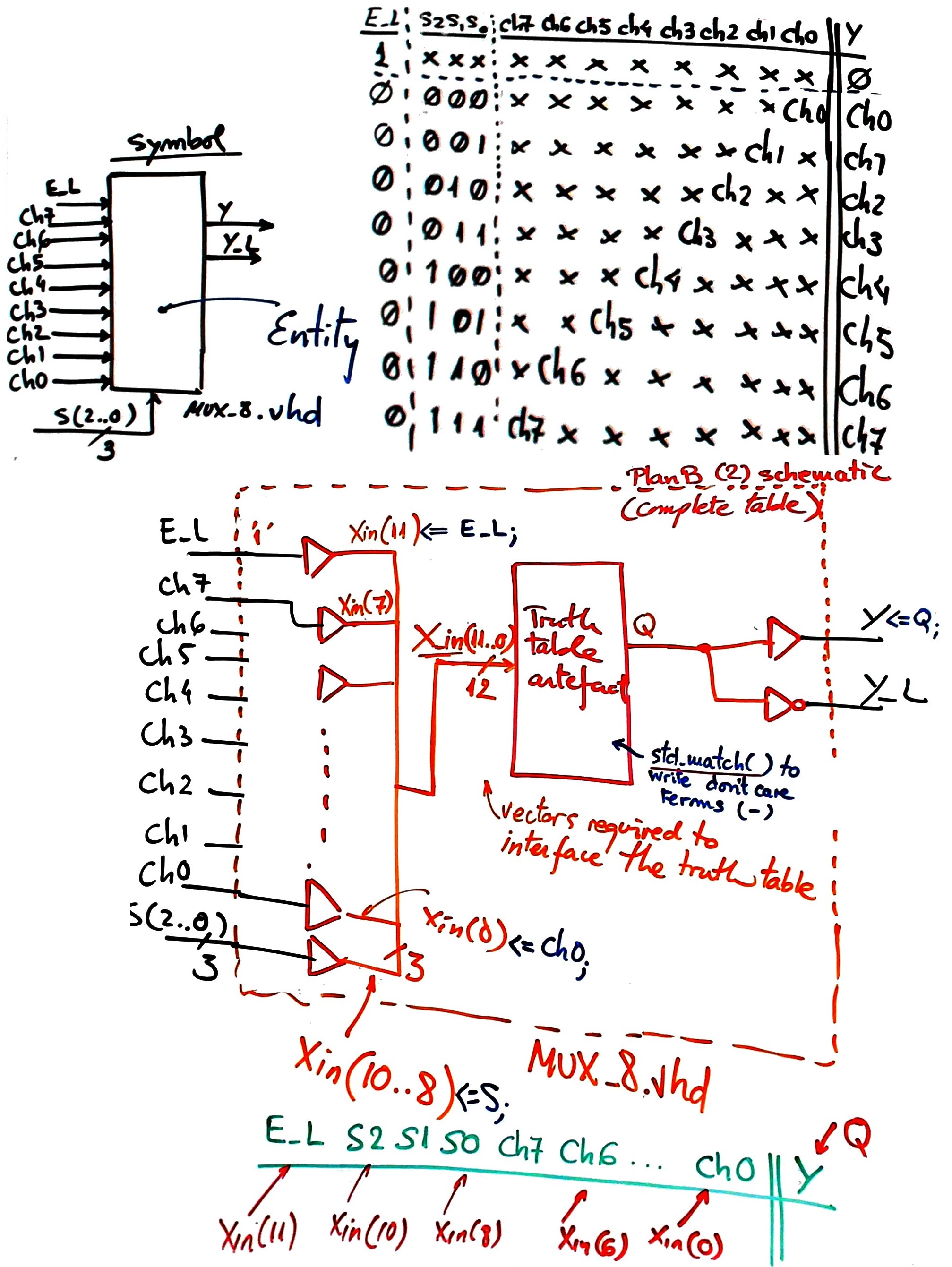
| Fig. 2. Symbol adapted from datasheets. A multiplexer is a data selector. |
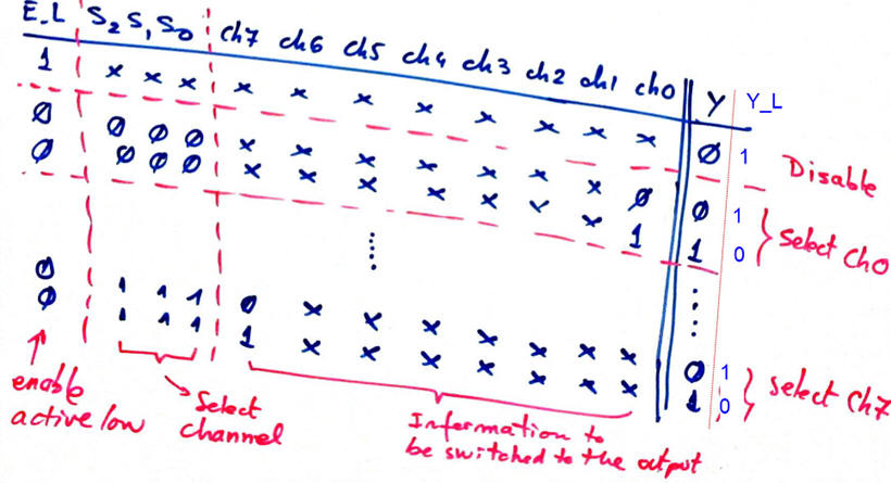
In Fig. 3 is represented the circuit's truth table.
|
|
| Fig. 3. Truth table. Twelve inputs means 4096 binary combinations. |
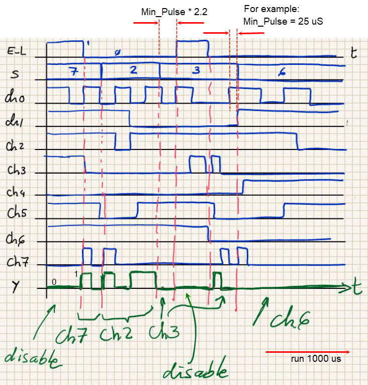
Finally, in Fig. 4 there is an sketch of a timing diagram.
|
|
|
Fig. 4. Example of a timing diagram sketch timing diagram to demonstrate how the circuit works for different inputs and so, be able to translate it later to VHDL as a testbench. |
Find and study similar products, like MUX_16, MUX_4, MUX_2 and also demultiplexers.
2. Planning
This is the general concept map rec. to design most of CSD circuits.
This flowchart explains the main concepts involved in VHDL design flow process using a single VHDL file (plans A and B).
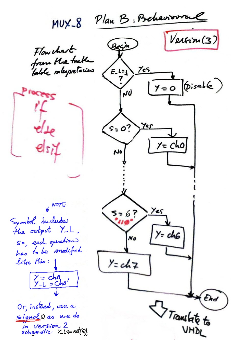
1. - Translate the truth table into an algorithm or flowchart.
 |
 |
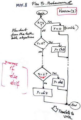 |
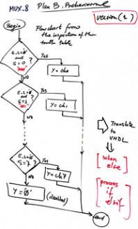
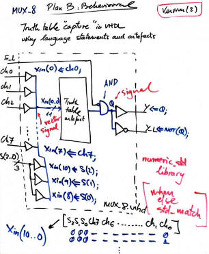
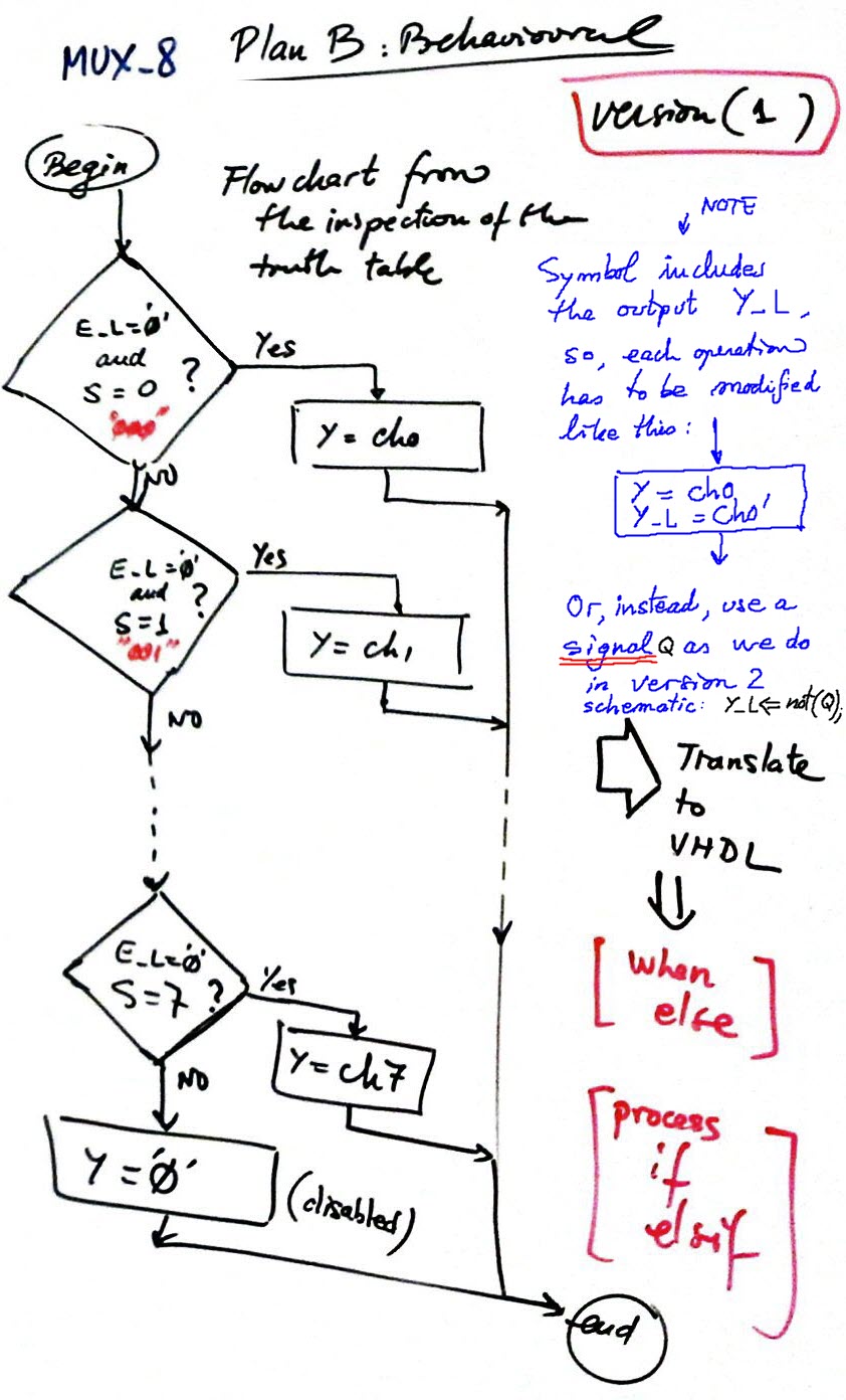
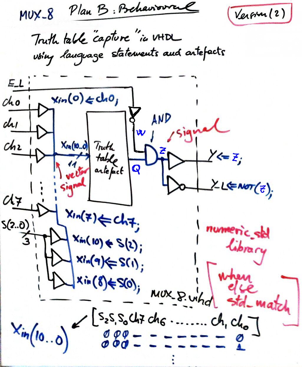
| Version (1) | Version (2) and (2_2) | Version (3) |
|
Fig. 5. Three versions of a plan B description. Versions 1 and 3 are flowcharts, and version 2 is an schematic that adapts the entire truth table artefact to input and output ports. |
||
2. - Save project files here (each behavioural description becomes a complete different project):
C:\CSD\P2\MUX_8_B1/(files)
C:\CSD\P2\MUX_8_B2_1/(files)
C:\CSD\P2\MUX_8_B2_2/(files)
C:\CSD\P2\MUX_8_B3/(files).
3.- Find a similar VHDL circuit with an architecture that corresponds to a truth table or algorithm to copy and adapt. Translate your algorith, flow chart or schematic into VHDL in a single file.
3. Development
Name the project MUX_8_prj and use one of the EDA tools to implement it selecting a target programmable chip (sPLD, CPLD or FPGA) from our laboratory training boards.
NOTE: Do not write VHDL code without the corresponding schematic / equation / diagram / flow chart / algorithm from the previous planning section. Here in CSD, VHDL source file is always a direct translation of your sketches represented in pen-and-paper. Submitted VHDL files, project developments and testing will not be marked unless they go accompanied byspecifications and planning discussion.
1.- Write VHDL files. The entity name is related to the symbol in Fig. 2. Note that in this project channel inputs are not considered a vector but individual wires.
NOTE: Use in CSD the Notepath++ enriched text editor, a very convenient free tool for writing VHDL and C files. Another editor is Scriptum from the company HDL Works.
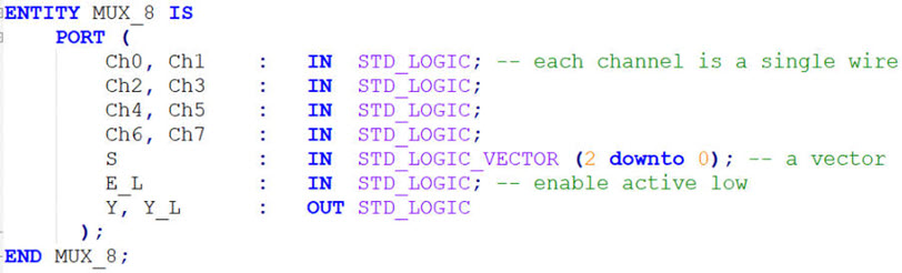 |
| Fig. 6. Entity descrition of the entity is the same for all design plans. |
These are up to four versions: (1) MUX_8.vhd; (2_1) MUX_8.vhd; (2_2) MUX_8.vhd; (3) MUX_8.vhd, accordingly to the plans infered above.
2.- Synthesise the circuit's architecture accordingly to the plans B:
Start an EDA tool project for a sPLD/CPLD/FPGA chip MUX_8_prj and obtain the synthesised circuit. It is a project consisting of a single VHDL file (flat design).
Print, analyse and comment the computer generated RTL and technology views or schematics of the circuits.
 |
| Fig. 7. Example of RTL. |
|
|
| Fig. 8. Example of technology view. |
Discuss the advantages and drawbacks of each development. Compare specifically the RTL and technology views of the several options for writing truth tables.
4. Testing
To test the solution whatever it is from plan A, plan B or plan C1 or plan C2, use the same test bench because even if you have different architectures, we use always the same entity definition under test. The testbench fixture containing the main ideas and concepts involved in this schematic is represented in Fig. 9.
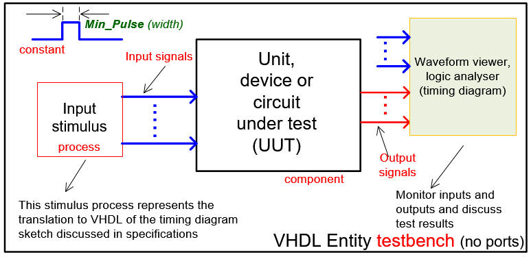 |
| Fig. 9. Testbench VHDL schematic. |
1.- Generate the template of the VHDL simulation testbench. The name of the file will be: MUX_8_tb.vhd (if the tool generates a MUX_8.vht, simply rename and copy it at project folder).
2.- Start an EDA VHDL simulator project to verify the Device-Under-Test (DUT) using a VHDL simulator test bench.
This is an example of testbench MUX_8_tb.vhd where inputs have been stimulated with logic values. Copy and paste to your design only constant Min_Pulse and input signals stimulus proces. Testbench VHDL simulation stimulus is the translation to VHDL of the timing diagram in Fig. 4.
3.- Start the simulation process with only a few input vectors (from the timing diagram sketch in the specifications) to see if the whole simulation process works and you are able to watch correctly input and output signals activity.
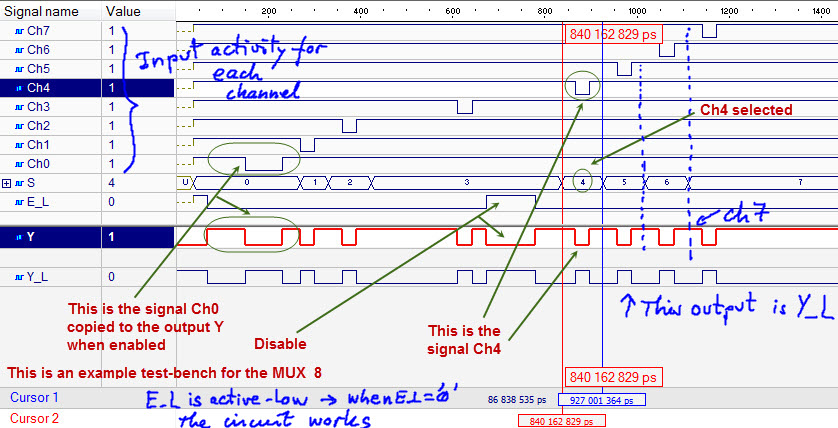
4.- Verify applying sufficient test vector that the device works as expected (verify how the information of each channel is selected). Print the timing diagram screen and add comments on the signals to show how the device works.
In Fig. 10 there is an example of commented test bench results from the logic analyser (wave) available in the EDA tool simulation tool. Use coloured pens.
 |
|
Fig. 10. Example of a timing diagram produced by the simulator with some mandatory comments and discussion on the way the circuit works. |
5. Report
6. Prototyping
| Home Term 23/24-Q2 Contact Products Electronic devices and companies Software Books Magazines Instruments DEE Library EETAC DEEL |

|
|
| Web activa des de 09/2001, @ F. J. Robert, J. Jordana. Web editat amb Microsoft Expression Web 4. El contingut és un complement als materials d'estudi del curs Circuits i Sistemes Digitals disponibles al campus digital Atenea. Llicència:Reconeixement 4.0 Internacional de Creative Commons |