|
|
Bachelor's Degree in Telecommunications Systems and in Network Engineering |
|
|
|
|||||
Chapter 3 problems |
- D3.23 - |
Earbuds control buttons (μC - C) |
|||
|
|
|||||
1. Specifications
Design the button decoder (BTN_cntl) that is typical in many commercial Bluetooth earbuds targeting a PIC18F4520 microcontroller chip. The idea is to assign a binary code to each function once detected. Fig. 1 shows a typical pair of commercial earbuds. Indeed, the final product for such space-constrained application, better be implemented in ultra-small 2 mm x 3 mm Dual Flat No-lead (DFN) 6-8pin package μC such PIC10L3xx or ATtiny102.
The same project designed using hardware is stated in D2.23.
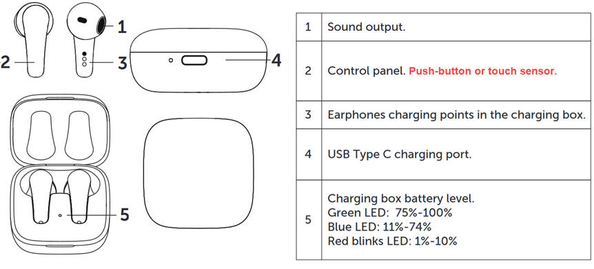 |
| Fig. 1. Example wireless commercial earbuds. Only one tactile pushbutton or capacitive touch sensor is available for commanding operations. |
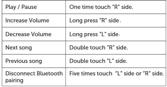
Once paired, depending on the apps selected in the mobile phone, earbuds can be used for answering phone calls, voice assistance or playing music. Functions assgned to short and long clicks depends on the model and the earbud branch. Let us consider option #1 simplified in Fig. 2 where only typical music player functions are listed.
Option #1 example functions and actions:
 a) |
| Fig. 2 a) Example especifications when used as music player. |
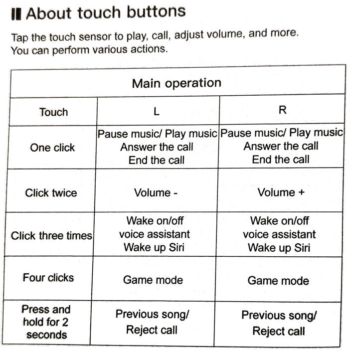
Option #2 example functions and actions for multiple applications: call, music, gaming.
 b) |
| Fig. 2b) Example especifications when used for phone, music and gaming apps. |
An internal switch S may be used to select left or right earbuds. For example S = '0' is the right earbud, S = '1' is the left earbud.
The idea is organise a FSM to detect one, two or five continuous short clicks, and also a long press. Fig. 3 shows a block diagram of an earbud from Toshiba company.
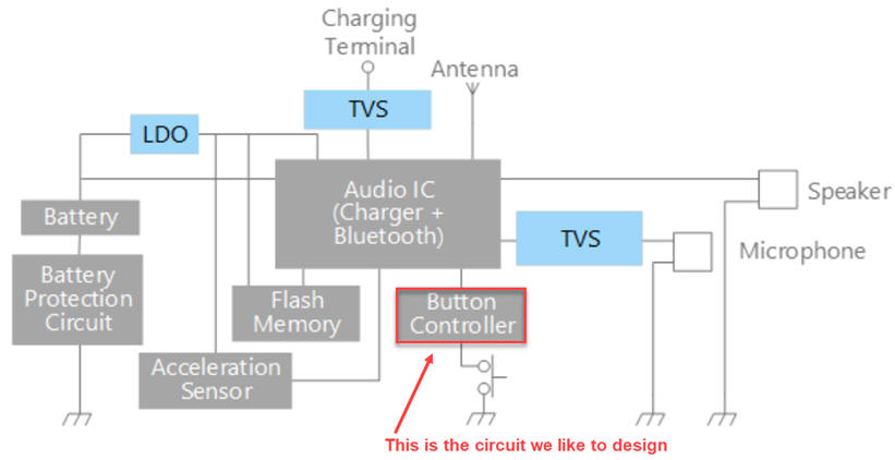 |
Fig. 3. Block diagram of an earbud. Reference paper: wireless earphone solution for long time operation with a small battery on a wireless earphone. TVS stands for transient voltage suppressor diodes to prevent the destruction of the electronics due to electrostatic discharges (ESD). LDO is a low dropout voltage regulator. |
Experiment in a protoboard and characterise the signals from a typical push-button. What is the typical time duration of a short and a long pulse?
2. Planning
Let us build the product organising several design phases, and several steps within each phase.
First of all, we have to imagine how the captured signal will look like. How many samples do you need to identify the three patterns. What is the typical short click duration? Draw some waveforms in a timing diagram as in Fig. 4.
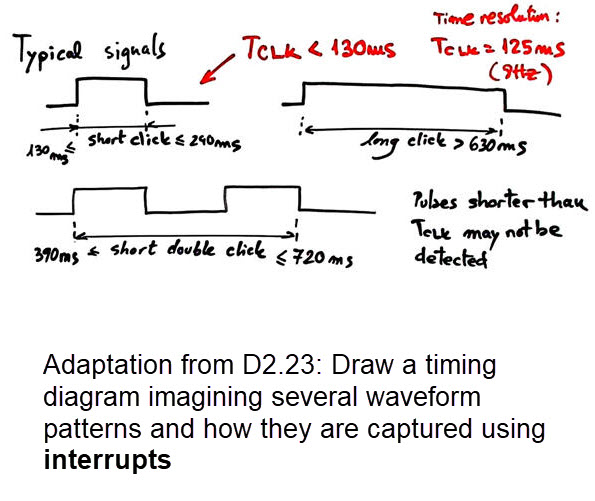 |
Fig. 4. We can consider that a single short pulse duration is between 130 ms and 240 ms, as we did in D2.23. And the same with the shape and duration of the other pulse pattersn of interest. We can imagine the same 8 Hz sampling frequency. Thus, a signal capture window of seven samples is required before analysing the waveform and deciding which function assign. Thus, in this project it is essential to simulate the signals in Proteus using the available pattern or digital generator. Use this file Click_pattern_generator.zip to learn how to use the pattern generator for simulations short and long clicks. |
An easy way to infer how the circuit may be conceived is to use an external interrupt INTx (x = 0, 1, or 2) to start the acquisition when the active PB rising edge is detected. Then, we can use an external CLK = 8 Hz (another INTx) to acquire the seven or eight samples reading the same PB value in order to generate the RAM variable var_CP (captured_pattern). Thus are the two external interrupt sources required all the time?
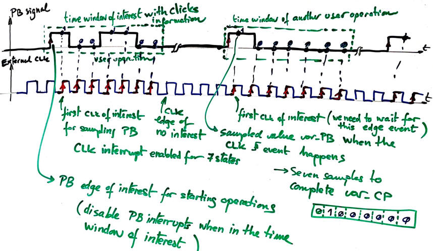 |
Fig. 5. This sketch is an analysis of what is of interest in this adaptation to solving D2.23 using microcontroller interrupts. We have to detect the first PB event (for instance a rising edge) to start the signal capture from an initial Idle state, and this is done well using external interrupts. Operations will start waiting for the first CLK event of interest (for instance the rising edge). This waiting time is variable, but less that 125 ms. Seven CLK interrupts will be required to complete the acquisition of the variable var_CP and continue the process compariong patterns captured. |
Design phase #1: basic features
Solve the circuit for the design step #1. Only when it is fully tested working correctly and reported, solve the design step #2.
Design step #1. Consider an initial circuit with no side S switch. Verify that the signal acquisition mechanism works.
Project location:
C:\CSD\P10\BTN_cntl_s1\(files)
Project source files:
BTN_cntl.pdsprj, BTN_cntl.c
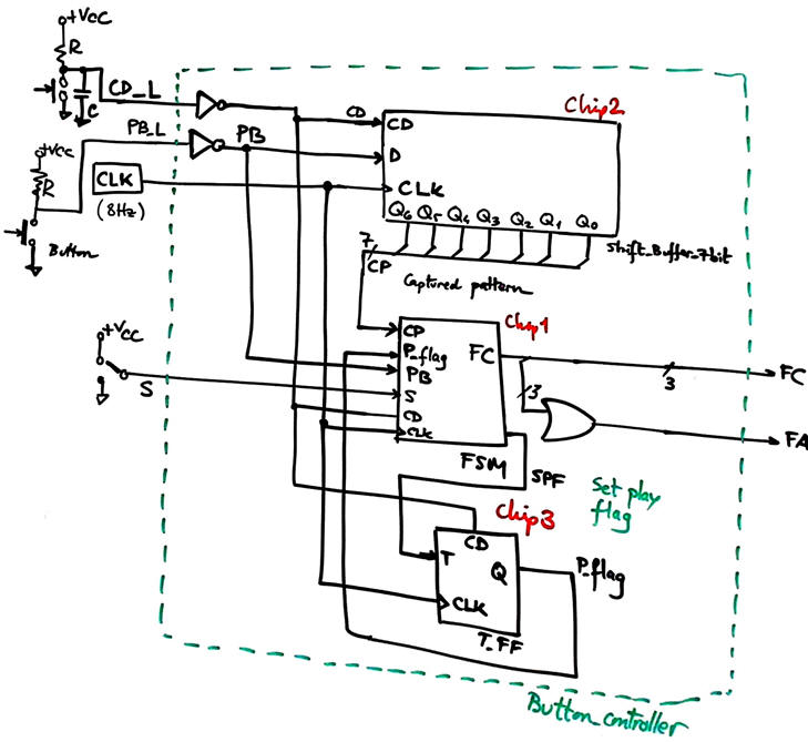
a) Draw the hardware schematic necessary for step #1. PB push button is replaced when simulating in Proteus by the pattern_generator using a rotary switch. CLK oscillator (8 Hz), output function code, function available, reset circuit MCLR_L, and an 12 MHz quartz crystal oscillator. Explain how to configure the inputs and outputs in init_system().
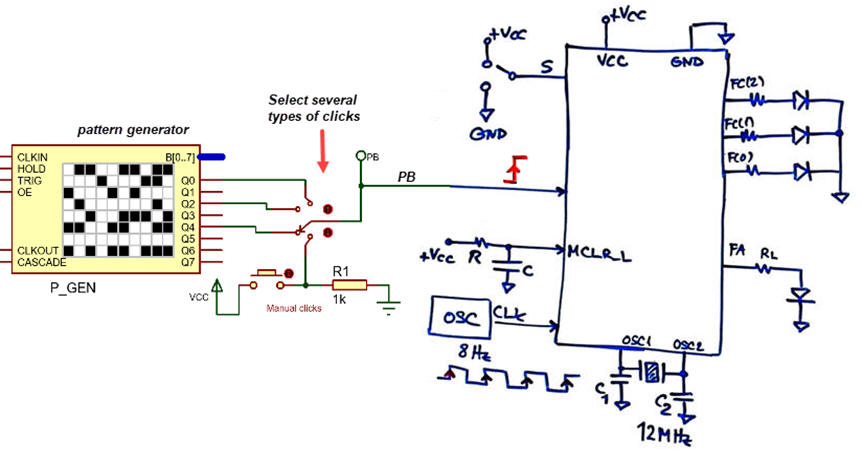 |
Fig. 6. Example of hardware circuit. You can choose the port pins to be read and written. Pay attention that PB and CLK must be connected to external interrupt pins. |
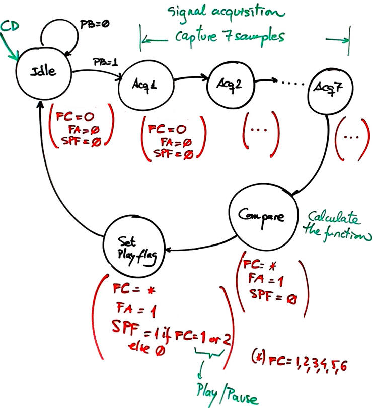
b) Draw the state diagram indicating how the state transitions will work. What outputs in each state?
- How to adapt the D2.23 Fig. 7 here? How to read the seven samples using a 125 ms delay between them? Where (in which place in the software) to shift and save the sampled PB values?
- What variables are required? What wil be the shift_register_7bits in D2.23 Fig. 6 here?
- What to do for watching always the last FC(2..0) vector lighting continuously in the LED until another pattern is processed?
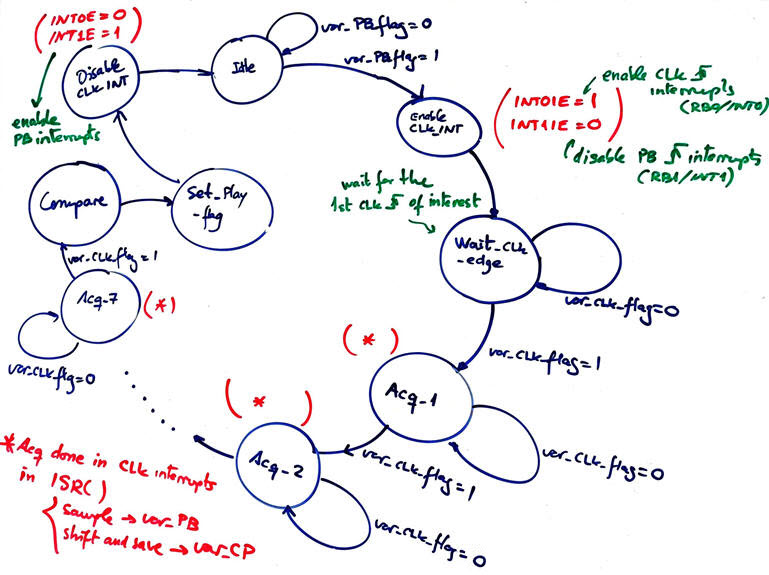 |
Fig. 7. Idea of state diagram controlled by interrupt variables. For most of the states only state transitions (state_logic()) are represented, discuss how to complete it using parenthesis for output_logic(). |
c) Draw the hardware/software diagram indicating the required RAM variables and how the FSM is solved in software.
- What variables are required? What wil be the shift_register_7bits in D2.23 Fig. 6 here?
- What wil be the T_FF to toggle play/pause in this adaptation?
- What signals wil be read (if any), when? Organise read_inputs().
- Organise write_outputs().
- The two interrupt sources, do they have to be enabled always? You can keep CLK interrupts disabled when in Idle state.
d) Draw the truth tables and their equivalent flowcharts for state_logic() and output_logic() functions.
e) What is the interrupt service routine ISR() used in this application? Draw its flowchart. In this problem this function is also used for sampling the PB and acquiring the clicks pattern information.
f) Develop and test (debugging) the project capturing the hardware circuit in Proteus and writing the C source code. Use the pattern generator to check that effectively several click shapes are identified. You must use the watch window to monitor RAM variables from the very beginning.
This is good time to check whether the 8 Hz sampling frequency is a good parameter or it must be adjusted to another value.
Check as well if push-button clicks are detected correctly.
Design step #2. Add the S switch to decode all the left and right functions.
Inherit the step #1 source hardware and software files into de new location.
Project location:
C:\CSD\P10\BTN_cntl_s2\(files)
Project source files:
BTN_cntl.pdsprj, BTN_cntl.c
a) Draw the hardware schematic necessary for step #2. Add the new switch and resistor for input S. Explain how to configure it in init_system().
Explain what is new in sections b), c), d), e), f)
Develop and test the new feature.
Let us add an LCD display as studied in P11 to this application. In this way, the LED pattern output FC(2..0) can be replaced by the LCD written message "Increase volume", "Play", etc.
Project location:
C:\CSD\P11\BTN_cntl_LCD\(files)
Project source files:
BTN_cntl_LCD.pdsprj, BTN_cntl_LCD.c
g) Enhance the schematic from the previous design phase #1 to include an LCD attached to port D as studied in tutorials.
h) Enhance the software and the source file to drive the LCD.
Develop and test the new feature.
Design phase #3: Using TMR2 peripheral subsystem.
Design step #1. TMR2 to replace the external sampling CLK
The external sampling CLK is replaced by the internal 8-bit TMR2 peripheral to generate interrupts (TMR2IF). Discuss the main features of this peripheral and its applications.
Project location:
C:\CSD\P12\BTN_cntl_LCD_TMR2\(files)
Project source files:
BTN_cntl_LCD_TMR2.pdsprj, BTN_cntl_LCD_TMR2.c
i) Calculate TMR2 parameters required to generate a CLK of 8 Hz (var_CLK_flag period = 125 ms) to acquired the pattern and run the machine replacing the external CLK signal.
Develop and test the new feature.
Design step #2. TMR0 to generate a sleep signal
j) Add a new TMR0 to generate a new switch off (sleep mode) signal after 1 min of inactivity.
Project location:
C:\CSD\P12\BTN_cntl_LCD_TMR2_TMR0\(files)
Project source files:
BTN_cntl.pdsprj, BTN_cntl.c
Develop and test the new feature.
Optional Design step #3. Keep visible the FC(2..0) information for 5 s using another timer before going back to Idle resetting the FC(2..0). In this way you can see the decoded pattern information statically represented in the LED for 5 s.
| Home Term 24/25-Q1 Contact Products Electronic devices and companies Software Books Magazines Instruments DEE Library EETAC DEEL |

|
|
| Web activa des de 09/2001, @ F. J. Robert, J. Jordana. Web editat amb Microsoft Expression Web 4. El contingut és un complement als materials d'estudi del curs Circuits i Sistemes Digitals disponibles al campus digital Atenea. Llicència:Reconeixement 4.0 Internacional de Creative Commons |