|
|
Bachelor's Degree in Telecommunications Systems and in Network Engineering |
|
|
|
|||||
Chapter 3 problems |
- D3.5 - |
Designing a LED lamp dimmer (μC - C) |
|||
|
|
|||||
1. Specifications
Luminaries work with high efficiency LED lamps and the light generated can be dimmed using a control circuit. A typical bulb is 12W, 12V, E27 screw fitting. To modulate the light intensity we can use simple pushbuttons or rotary knots.
The same project designed using hardware is stated in D2.5.
 |
|
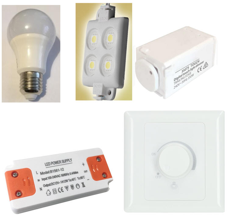
Fig. 1. Examples of luminaries, bulbs, dimmer circuits and power drivers. |
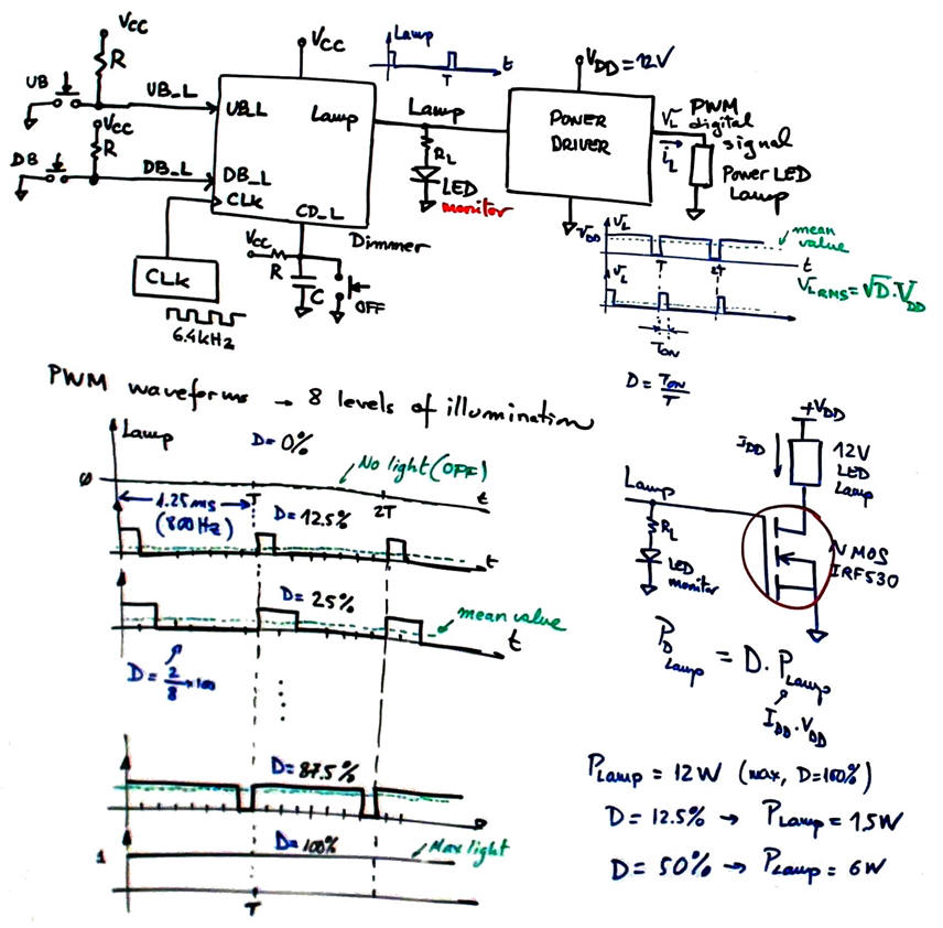
Let us propose the basic circuit for a dimmer in Fig. 2. Light intensity can be set in eight levels. Clicking button up (UB) light will increase, and clicking button down (DB) light will decrease. The idea behind controlling electrical power applied to a load like a LED bulb is to use digital pulsed width modulated waveforms (PWM). If the switching frequency is high, the eye will not be affected by flickering.
Let us invent a circuit capable of generating a 800 Hz PWM signal (T = 1.25 ms) with duty cycle modulations (D%) of 0, 12.5, 25, 37.5, 50, 62.5, 75, 87.5, 100.
 |
|
Fig. 2. Symbol and connection to a power lamp driver. |
The lamp power driver can be modelled in Proteus using power MOS transistors. At this initial phase a simple standard LED can be used to monitor the light intensity or brightness generated at the Lamp output.
2. Planning
Let us build the product organising several design phases, and several steps within each phase.
Design phase #1: basic features.
Solve the circuit for the design step #1. Only when it is fully tested working correctly and reported, solve the design step #2.
- Design step #1. Consider an initial circuit with only the up button UB.
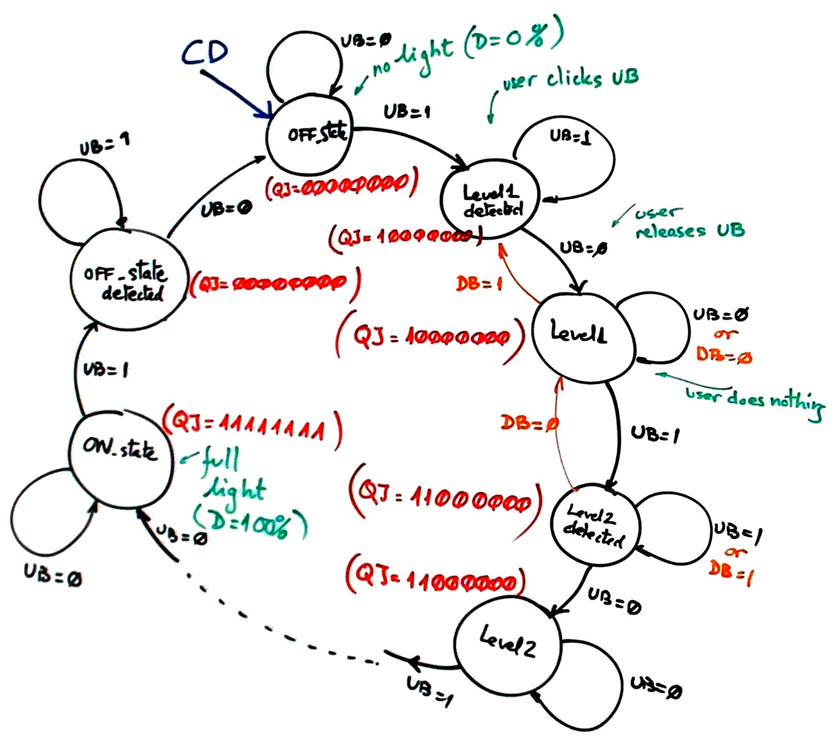
Firstly you can imagine how to generate a Johnson counter that goes up every time the external push-button UB_L is clicked. We need to use an external interrupt INTx (x = 0, 1, or 2) so that the level_detected_i states in D2.5 Fig. 6 are not required. You can use 8 external LED to visualise the code or, instead, even better you can use the watch window to monitor the current value of RAM variable var_QJ in memory.
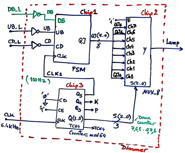
Secondly, you can generate a new external waveform at output Lamp imagining a datapath for shifting or multiplexing the current Johnson code value in var_QJ. This waveform will have a frequency of 800 Hz. Use another external interrupt as a CLK. These are some initial ideas for programming the MUX_8 function in D2.5 Fig. 3 as a shift register that works continuously in the main loop. In a similar way, you can simply program the functionality of the MUX_8.
Project location:
C:\CSD\P10\Dim_s1\(files)
Project source files:
Dim.pdsprj, Dim.c
a) Draw the hardware schematic necessary for step #1. UB_L push button, CLK push button or oscillator (800 Hz), Johnson code outputs, reset circuit MCLR_L, and an 8 MHz quartz crystal oscillator, Lamp output. Explain how to configure the inputs and outputs in init_system().
What pins will be read, if any? What variables will be written at a port pin? How many external interrups are required in this step#1?
b) Draw the state diagram indicating state transitions and outputs.
What example tutorial can be used as a model to copy and adapt?
c) Draw the hardware/software diagram indicating the required RAM variables and how the FSM and shift operations (datapath) solved in software.
d) Draw the truth tables and their equivalent flowcharts for state_logic() and output_logic() functions.
e) What is the interrupt service routine ISR() used in this application? Draw its flowchart.
f) Develop and test (debugging) the project capturing the hardware circuit in Proteus and writting the C source code. You must use the watch window to monitor RAM variables from the very beginning.
- Design step #2. Add the down button DB_L to control the light intensity in the other direction.
Inherit the step #1 source hardware and software files into de new location.
Project location:
C:\CSD\P10\Dim_s2\(files)
Project source files:
Dim.pdsprj, Dim.c
a) Draw the hardware schematic necessary for step #2. Add the push-button and resistor for input DB_L. Explain how to configure it in init_system(). A new external interrupt will be required (var_DB_flag).
Explain what is new in sections b), c), d), e), f)
Develop and test the new feature.
Thinking about the project, an optional feature in this phase #1 is to visualise the current value of var_QJ in an array of eight LED, so the user has a visual representation of the level of light intensity. Such circuit is replaced by the LCD in phase #2 to show the same information as a text message.
Another optional feature, may be to add a switch light control enable (LCE) to block the up and down push-buttons when high to generate a continuous 50% waveform. As you see, in these practical applications there are are always new features to add to the final product.
Let us add an LCD display as studied in P11 to this application. The idea is to use several ASCII characters to represent lamp illumination information
Project location:
C:\CSD\P11\Dim_LCD\(files)
Project source files:
Dim_LCD.pdsprj, Dim_LCD.c
g) Enhance the schematic from the previous design phase #1 to include an LCD attached to port D as studied in tutorials.
h) Enhance the software and the source file to drive the LCD.
In this design phase you can learn the LCD interface step by step. For instance:
Design step #1. Print ASCII messages on the LCD. For instance "MAX", "Minimum light", etc.
Design step #2. Print numeric information, for example the current duty cycle percentage "Light DC = 87.5%"
Develop and test the new feature.
Design phase #3: Using TMR2 peripheral subsystem.
The 800 Hz external CLK is replaced by the internal 8-bit TMR2 peripheral to generate interrupts (TMR2IF). Discuss the main features of this peripheral and its applications.
Project location:
C:\CSD\P12\Dim_LCD_TMR2\(files)
Project source files:
Dim_LCD_TMR2.pdsprj, Dim_LCD_TMR2.c
i) Calculate TMR2 parameters required to generate the same Lamp output frequency of 800 Hz (this Lamp waveform is generated serialising 8 bits at var_CLK_flag period Tp = 156.25 ms). In this way the external CLK signal can be eliminated and the application runs in the same way.
j) Add a new switch SP (speed) to be able to select between two different Lamp periods: 1.25 ms (800 Hz) and 2.5 ms (400 Hz).
Develop and test the new feature.
| Home Term 24/25-Q1 Contact Products Electronic devices and companies Software Books Magazines Instruments DEE Library EETAC DEEL |

|
|
| Web activa des de 09/2001, @ F. J. Robert, J. Jordana. Web editat amb Microsoft Expression Web 4. El contingut és un complement als materials d'estudi del curs Circuits i Sistemes Digitals disponibles al campus digital Atenea. Llicència:Reconeixement 4.0 Internacional de Creative Commons |