|
L1.2: Logic gates P1 analysis AND, OR, NOT, XOR, NOR, NAND, NXOR |
[10/9] |
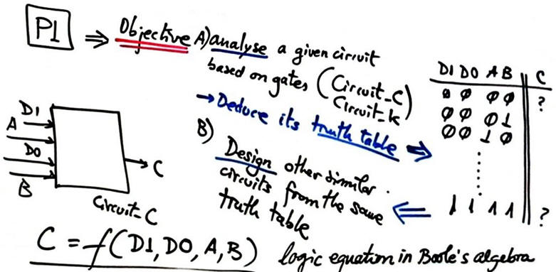
Specifications
Analyse the highlighted Circuit_C proposed in P1 to deduce its truth table.
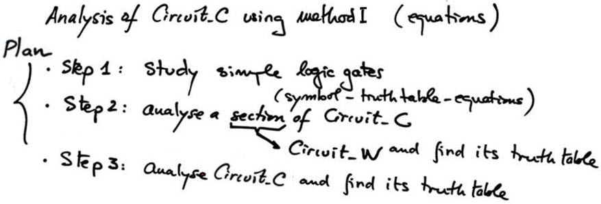
Planning
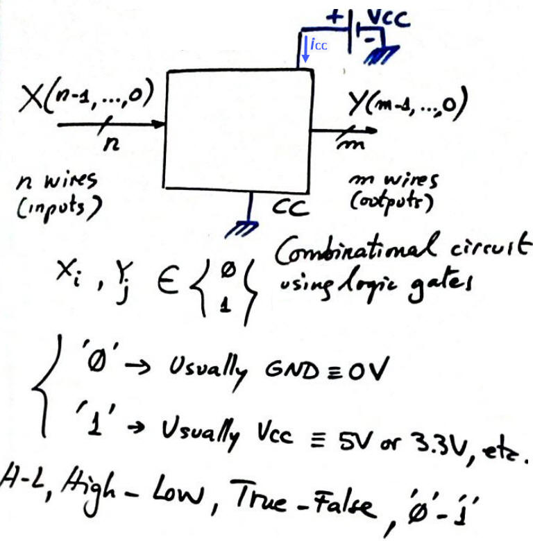
General combinational circuit symbol:
Step 1
1.3. Logic gates
1.3.1. Symbols
1.3.1.1. Buffer (non-inverter)
1.3.1.2. Inverter (NOT)
1.3.1.3. AND, NAND
1.3.1.4. OR, NOR
1.3.1.5. XOR, NXOR
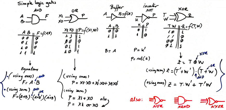
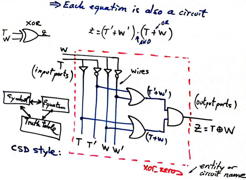
Standard logic gates: symbols, equations, truth table, product of maxterms and sum of minterms rec. 1, rec. 2. The concept of a logic gate represented in two complementary ways (schematic/symbol/logic diagram and logic equation) and its truth table to describe its specifications or how does it work.
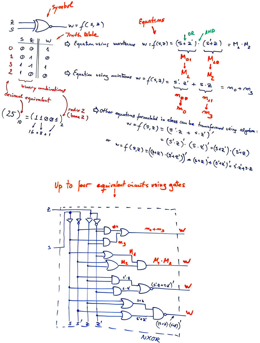
This below is another example on how a NXOR truth table can be realised using up to four different and equivalent equations:
1.3.2. Equations in boolean algebra, also from this reference: Ercegovac, M., Lang, T., Moreno, J. H., Introduction to digital systems, John Wiley & Sons, 1999, link (chapter 2, lecture viewgraphs).
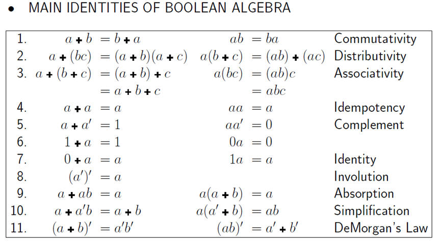
And also: x = (x + y) · (x + y') x = x · (y + y')
1.3.3. Truth table and canonical forms
1.3.3.1. Sum of minterms.
1.3.3.2. Product of maxterms
1.3.4. Timing diagrams
This reference explains content on logic gates and combinational circuits.
You can read books on the subject or browse the Internet searching the basic theory on digital electronics. For instance, here there is a series of 14 introductory videos to our subject (Dunn, K., Bluegrass Community and Technical College). Some of the videos also include "pdf" notes and exercises and additional web references.
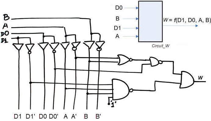
Exercise: Using equations from logic gates, find the circuit equation of the Circuit_W below: the algebraic notation that is totally equivalent to the schematic. Discuss your results with your class mates, it has to be the same equation for all of you.
