|
|
Bachelor's Degree in Telecommunications Systems and in Network Engineering |
|
|
|
||
|
|
Dual_MUX_4 plan A: structural single-file VHDL (flat) |
|
|
|
||
Type 74HCT153 standard commercial chip
1. Specifications
Design a classic chip like the 74HCT153 using plan A structural approach.
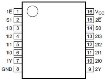 a) a) |
Fig. 1. a) Case and pin naming and enumeration of a classic 74HCT153 chip. We will interpret it as shown in b). Vector data select S(1..0) may be represented in binary radix-2 or as an unsigned decimal. Symbol name is Dual_MUX_4 meaning that data input channels and output are dual, they have two-bit size Ch0 --> Ch0(1..0). In other applications we may have other expanded devices like Octuple_MUX_8, meaning that Channel size is 8-bit for instance Ch0(7..0), and select channel is S(2..0) to be able to switch 8 data channels . Enable is active-low (E_L) meaning that the chip operates when E_L = '0'. |
b)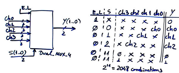 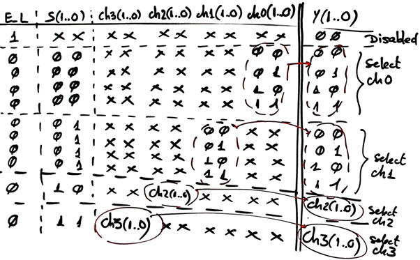 |
|
|
- How many maxterns does Y(1)
contain? |
|
Draw the sketch of a timing diagram to demonstrate how the circuit works for several input stimulus.
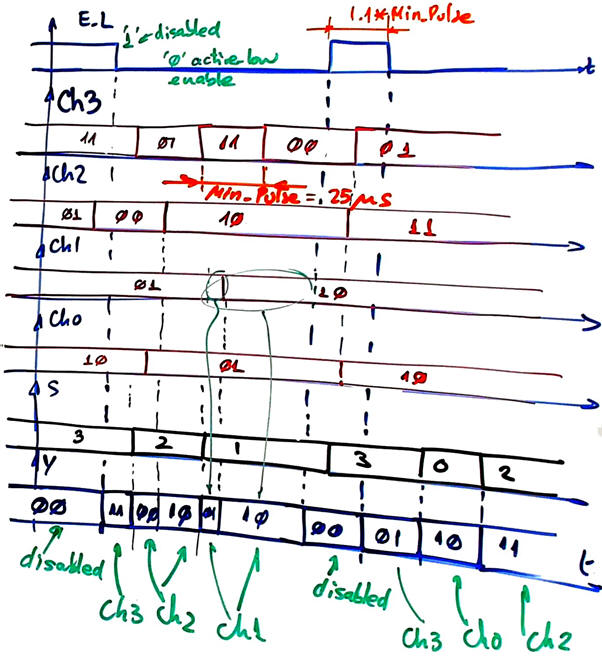 |
Fig. 2. Example timing diagram. |
2. Planning
Write minimised (SoP or PoS) equations using Minilog.exe for Y(1) and Y(0). For instance: truth table Dual_MUX_4.tbl and solution: Dual_MUX_4_corrected.txt.
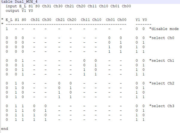  |
| Fig. 3. Truth table in minilog format and result represented in PoS equations. |
Project and file locations:
C:\CSD\P2\Dual_MUX_4_A/(files)
3. Development
Find a similar VHDL description for a plan A circuit, copy and adapt. Dual_MUX_4.vhd
This is the description of the entity accordingly to the CSD input and output naming.
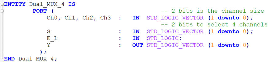 |
| Fig. 4. Entity definition is the same whatever the plan. |
Start an EDA synthesis project named Dual_MUX_4_prj for a given target chip, for example Intel CPLD EPM2210F324C3 and examine results.
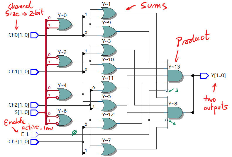 |
Fig. 5. RTL schematic of Dual_MUX_4 using structural description in SoP. |
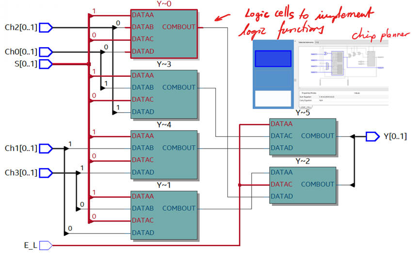
Technology view schematic.
 |
|
Fig. 6. Technology view of Dual_MUX_4 targeting Intel CPLD: EPM2210F324C3. The Chip Planner tool in Quartus Prime can be used to locate exactly where your circuit is synthesised in the CPLD lattice of logic cells. |
4. Testing
In Fig. 7 is represented the testbench schematic to stimulate the unit under test (UUT) with input vectors. Generate the skeleton of the testbench file and add stimulus translating to VHDL input activity from the time diagram in Fig. 2. This is an example of a simple test bench Dual_MUX_4_tb.vhd where the inputs have been stimulated with logic values.
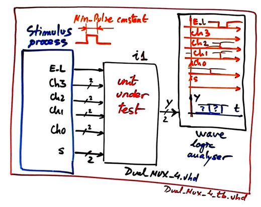 |
Fig. 7. Testbench fixture to verify that our circuit works as expected. |
Start the VHDL simulator project, Dual_MUX_4_functional_sim, and run the test. Verify applying sufficient test vector that the device works as expected (verify how the information of each channel is selected). Print timing diagram screen and add comments on the signals to show how the device works.
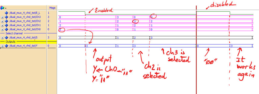 |
| Fig. 8. Waveform results from the logic analyser. |
5. Report
6. Prototyping
| Home Term 24/25-Q1 Contact Products Electronic devices and companies Software Books Magazines Instruments DEE Library EETAC DEEL |

|
|
| Web activa des de 09/2001, @ F. J. Robert, J. Jordana. Web editat amb Microsoft Expression Web 4. El contingut és un complement als materials d'estudi del curs Circuits i Sistemes Digitals disponibles al campus digital Atenea. Llicència:Reconeixement 4.0 Internacional de Creative Commons |