|
|
Bachelor's Degree in Telecommunications Systems and in Network Engineering. Bachelor's Degree in Aerospace Systems Engineering |
|
Laboratory 1. Software installation. Lab instruments Instruments and probes. EDA tools. Electronic circuits simulation using Proteus |
Objectives |
EDA installation |
Probes |
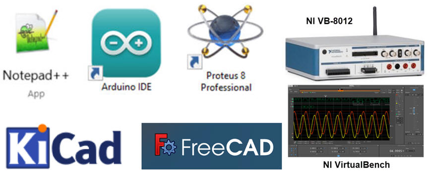
(1) Install and license commercial software: Proteus and NI VB-8012 VirtualBench in your portable computer.
(2) Install free apps: KiCad, FreeCAD, Arduino IDE.
(3) Install an enriched text editor such Notepad++.
|
|
|
Fig. 1. Software applications icons. |
(4) Run demonstration applications to check that the software is installed and operating correctly.
(5) Modelling probes and study how to represent the equivalent circuit of typical instrumentation. Measuring voltages, currents. Bandwidth.
This is an individual laboratory, each student must have the specified EDA tools running correctly in its portable computer.
Objectives |
EDA installation |
Probes |
Install Proteus
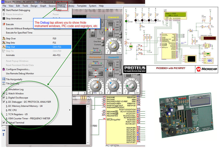
1. Install Proteus as indicated using our cloud license server.
Test
Once installed, most of the applications contain demo designs and projects that can be used for verifying that the software works correctly.
|
|
|
Fig. 2. Example of hardware and software project development and debugging environment in Proteus, simulating Microchip PICDEM2 training board. |
Install Arduino
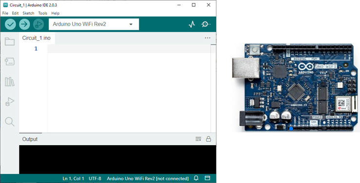
2. Download and install the default Arduino integrated development environment (IDE).
|
|
|
Fig. 2. Arduino IDE opening window. The current version is 2.3.2. |
Test
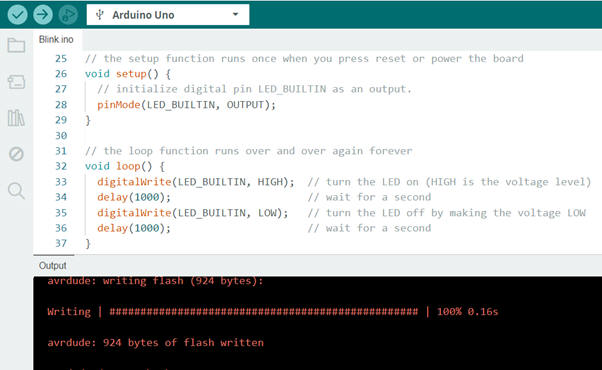
Run the blinking LED source code and program the Arduino board to check that the application is correctly installed.
|
|
|
Fig. 3. Arduino running a program after uploading the board. |
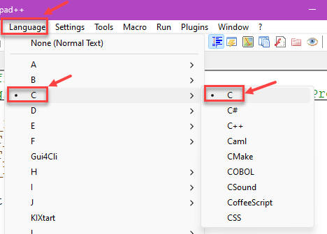
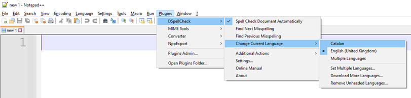
Install Notepad++
3. Install Notepad++. Select C language. You can also install a plugin for detecting spelling errors in several languages.
|
|
|
Fig. 3. Notepad++ and its spelling checker plugin. |
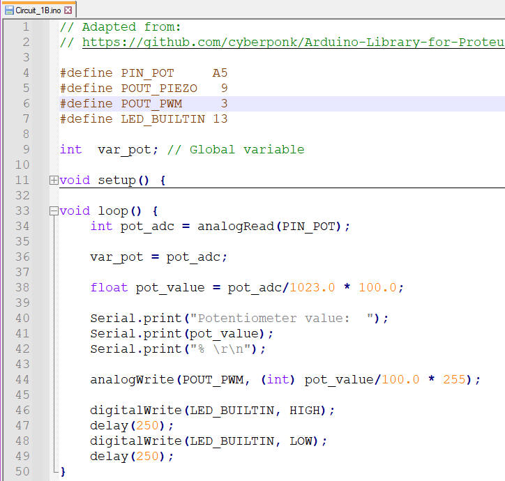
Test
Load a C or Arduino source file, select the language, and check that the text is coloured as shown in Fig. 4.
|
|
|
Fig. 4. Enriched text editor. |
Install KiCad
4. Install KiCad for simulation, schematic capture and PCB design. Install FreeCAD for building or adjusting 3D component models associated to footprints.
Prototyping using training boards is the previous step before designing custom printed circuit boards (PCB).
|
|
|
Fig. 10. Example: basketball scoreboard system prototype. |
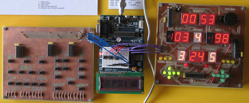
Find similar examples of prototypes in internet.
Prototyping is practised all the time when using Arduino and other training boards environments. As an example browse this page on Arduino Prototype to Manufacturable PCB: An LED Multiplexer, by Thomas Nabelek, 2016.
Alternative UPC-licenced EDA software for the same purpose is Multisim and Ultiboard (NI-Emerson) or Fusion-360 (Autodesk). Other commercial professional EDA that include academic plans are: OrCAD (Cadence), eCADSTAR (Zuken), Altium Designer, Proteus PCB software (Labcenter).
Install NI-VB8012
5. Install VB8012 Virtual Bench instrument driver.
|
|
|
Fig. 4. With NI license manager you can activate your NI software using our UPC licenses. |
Testing
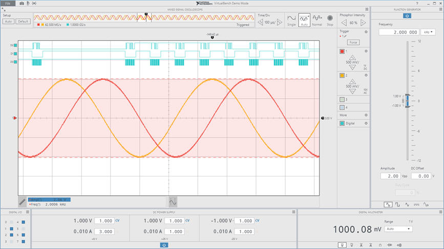
Check that the appications detects the USB instrument and characterise and print an acquisition of the reference squared signal.
|
|
|
Fig. 9. Square wave reference signal. |
Activities:
Doing LAB1 means having been able to install, license and run the EDA tools in your portable computer. For each tool, print a sheet of paper containing images from the installation.
NOTE: Be aware that for printing in paper instrument captures, diagrams, code, etc. you must change the black background colour to white so that your printed does not waste ink.
Objectives |
EDA tools installation |
Oscilloscope probes |
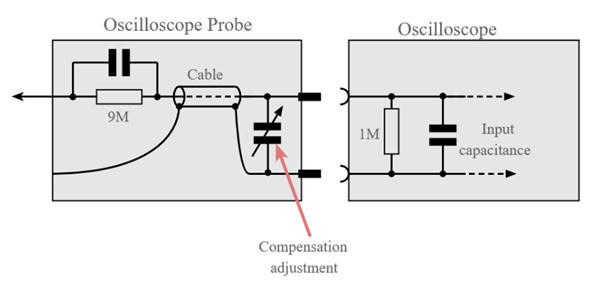
Modelling and using oscilloscope probes.
|
|
Fig. 1. The electrical equivalent of an oscilloscope measurement probe. (picture ref.). |
Draw the electrical equivalent circuit of the function generator connected to the oscilloscope using a probe. Find in datasheets and user guides the capacitor values (for instance the PS2150 probe))and calculate at which sinusoidal frequency the voltage at the oscilloscope drops 3 dB for the probe at a) 1:1 and b) 10:1.
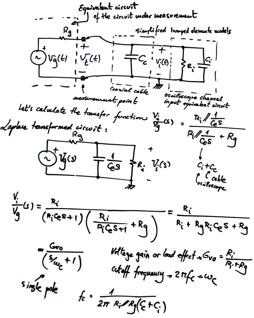
a) Passive probe 1:1. Voltage gain (attenuation) and -3 dB bandwidth (BW).
|
|
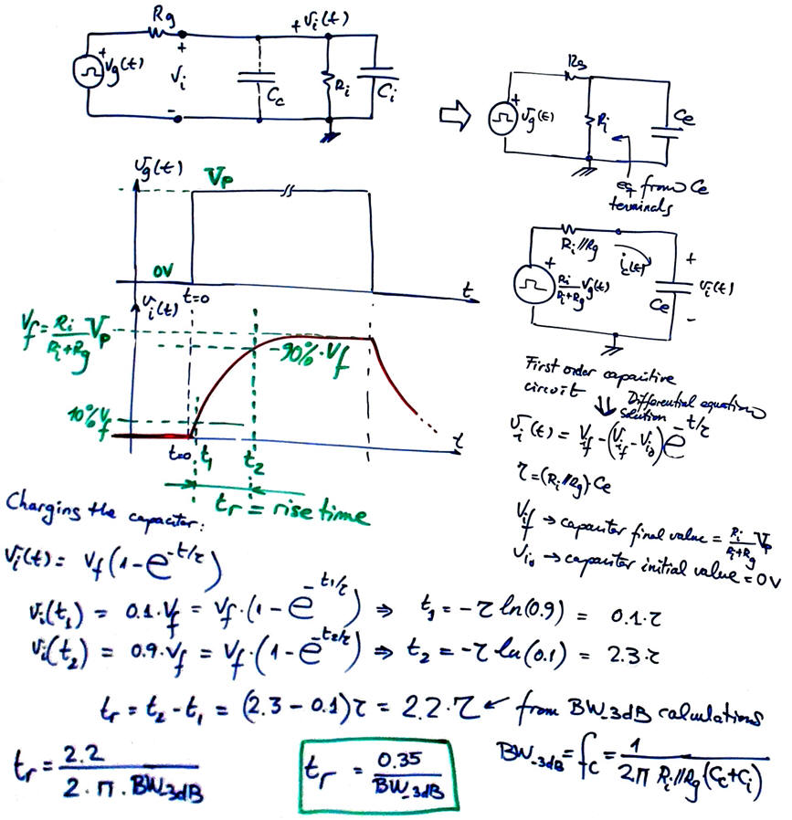
Fig. 2. Bandwidth calculation for the 1:1 probe, basically a simple coaxial cable. |
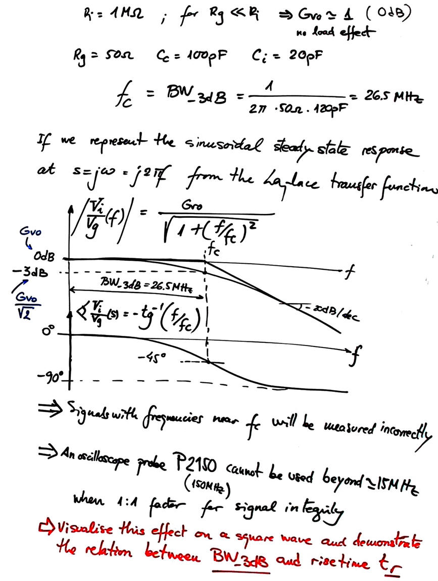
Demonstrate the formula relating BW-3dB and rise time.
|
|
Fig. 3. Rise time and BW-3dB relation modelling a capacitive first order simple RC circuit at the oscilloscope input. |
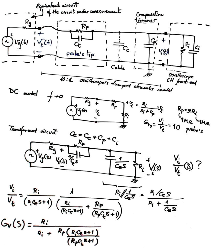
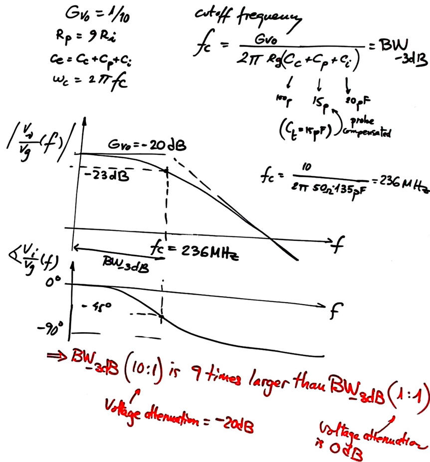
b) Passive probe 10:1. Voltage gain (attenuation) and -3 dB bandwidth (BW).
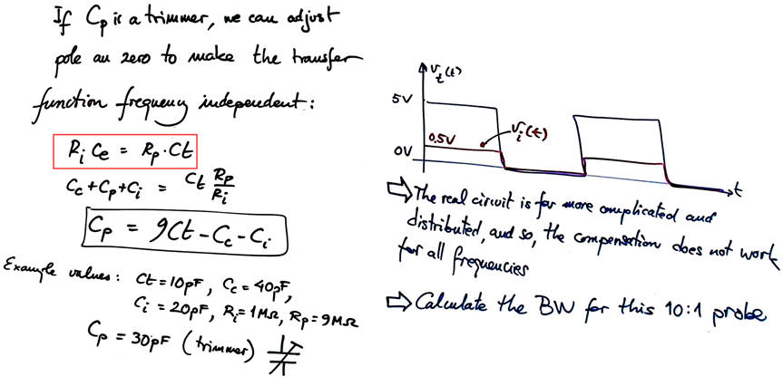
Calculate components and trimmer values for compensating capacitive effects over frequency. Use real data from probe datasheets to generate values.
|
|
Fig. 4. Approximate equivalent circuit and analysis of a typical passive prove in 10:1 configuration. |
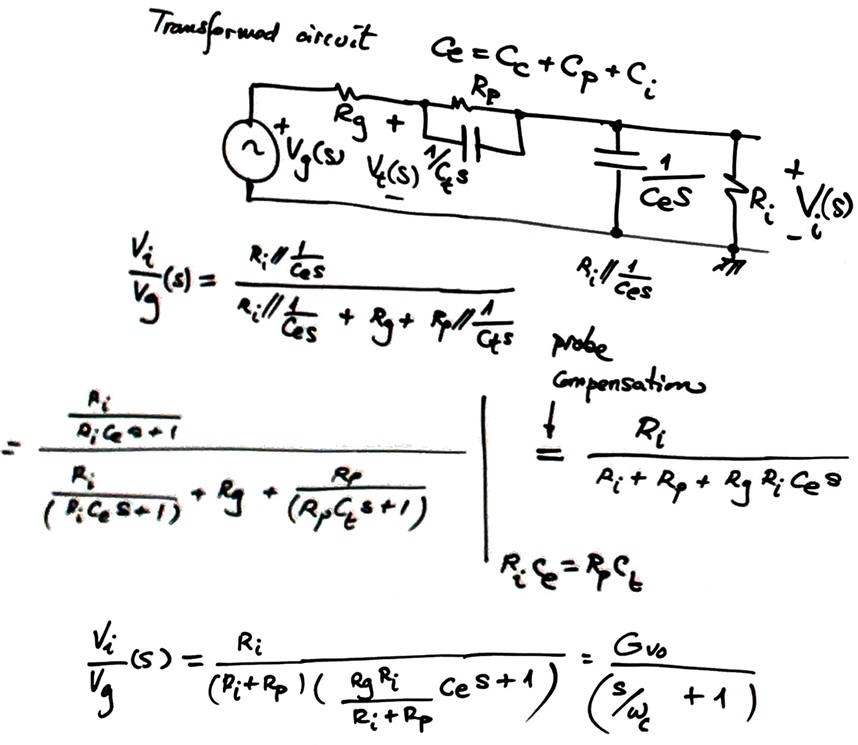
Calculate the 10:1 probe new bandwidth (BW-3dB) and compare with probe 1:1
|
|
| Fig. 5. Bandwidth calculation for the 10:1 probe modelling the same first order capacitive circuit. We pay the price of derating the voltage gain from 0 dB to -20dB, but we can use the probe at much larger frequencies. |
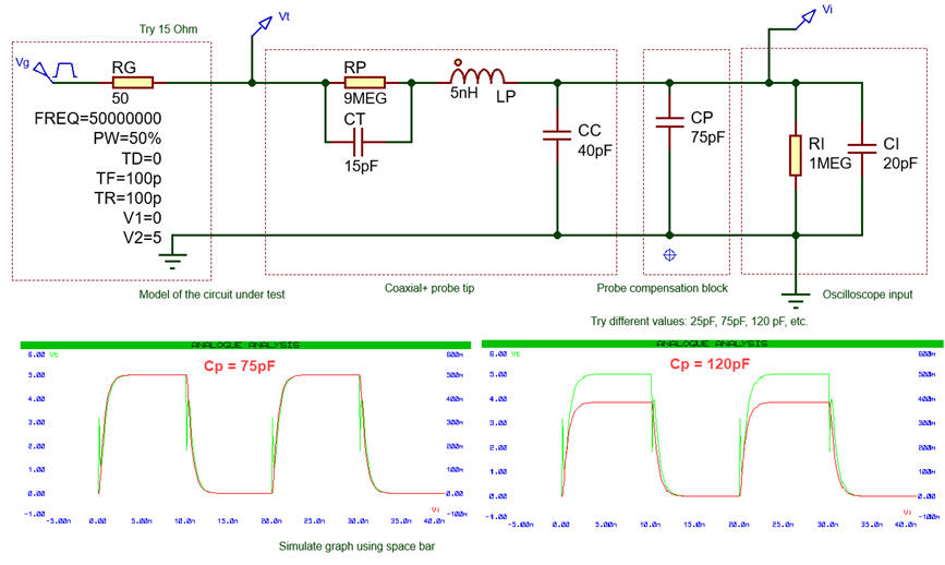
Example verification simulations using Proteus. Here it is easy introducing second order effects like wire parasitic inductances (LP) and visualise what happens when modelling 10:1 and 1:1 probes, using both sinusoidal and pulsed waveforms.
Do not start a circuit from scratch but use and adapt this sample oscilloscope_probe.pdsprj.
|
|
|
Fig. 6. Example of simulation trimming the compensation capacitor CP in the probe block. Try CP = 75 pF, Rg = 1 W. Try LP = 10 pH (practically zero inductive effect) and observe the waveforms. |
Experimentation and measurements
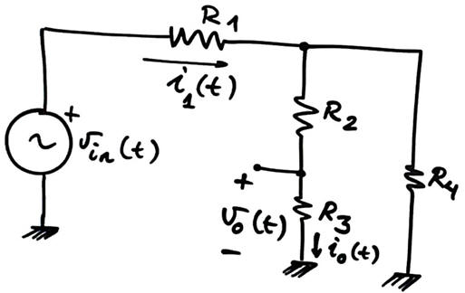
Consider measuring v0(t) and i0(t) in the Fig. 7 circuit using an oscilloscope. Use (a) ideal probe, (b) 1:1 probe, (c) 10:1 probe. Apply simplifications, equivalent models or whatever techniques you remember from previous subjects. Calculate the relative error for each probe.
w = 2pf; f = 1 MHz.
option #1: vin(t) = VA sinwt; VA = 5 V; R1 = 300 W; R2 = 820 W; R3 = 1.8 kW; R4 = 2.7 kW
option #2: vin(t) = VA sinwt; VA = 3.3 V; R1 = 47 W; R2 = 86 W; R3 = 180 W; R4 = 330 W
|
|
Fig. 7. Circuit with resistors for measuring using probes. |
| Home Contact Electronic devices and companies Books Magazines Instruments Digsys Library EETAC DEEL |

|
|
| Web activa des de 01/2023, @ F. J. Robert. Web editat amb Microsoft Expression Web 4. El contingut és material de referència per al disseny d'equips electrònics. Llicència:Reconeixement 4.0 Internacional de Creative Commons |