|
|
Bachelor's Degree in Telecommunications Systems and in Network Engineering |
|
| | ||
SP2_4: Implementing counters and registers |
||
|
| ||
| NOTE: This subproject must be solved only after having completed successfully lab session Lab7 because you will copy and adapt materials from it. |
1. Specifications
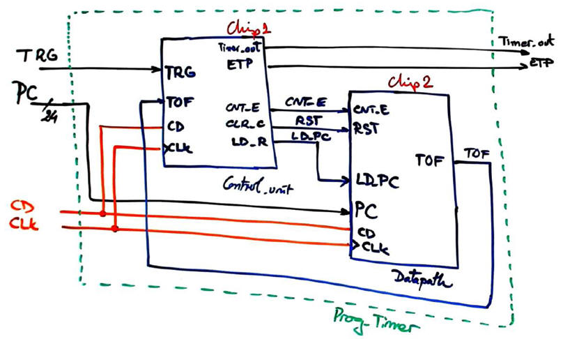
Objective: Design the datapath (Chip2) component of the Prog_Timer using the internal architecture proposed in Fig. 2.
-
Comp_24bit was designed in SP2_1.
-
Counter_mod16M can be designed using either plan Y (single-file) or plan C2 based on Counter_mod16 components. Use this project for discovering such solutions.
-
Data_reg24bit can be designed using either plan Y (single-file) or plan C2 based on Counter_mod16 or Data_reg_4bit components. Use this project for discovering such solutions.
 |
|
Fig. 1. Datapath component becomes the Chip2 in the Prog_Timer dedicated processor architecture. |
2. Planning
This is the proposed architecture based on plan C2 using several components and signals. Observe how all the wires, even the unconnected has to be given a name for proper translations to VHDL.
 |
|
Fig. 2. Datapath internal architecture based on memory and operational resources such counters, registers and arithmetic combinational circuits. |
-
Comp_24bit was designed in SP2_1. However, this is the time for finding new approaches for the internal design of components. For example, how can you design a "tree comparator" that is faster than the typical ripple comparator?
-
Because the lab group have two o three members, it is possible to design Counter_mod16M using the several plans proposed and discuss differences (at least in this planning section).
-
And again, this is the time for you to try to design the Data_reg24bit using the several plans proposed and discuss differences (at least in this planning section)..
Project and file location:
C:\CSD\P_Ch2\SP2_4\
3. Developing
Translate one plan for each component to VHDL and start a synthesis project for a given target chip.
Print and discuss RTL and technology views.
Deduce the number of registers used in the datapath component.
4. Functional testing
For this project, due to its complexity, let us not to test it now because there is too much work organising the many stimulus signals generated by the FSM. Therefore, we propose to complete and develop P_Ch2 and check it all using only TRG button and PC values.
5. Gate-level testing
The same indication in 4. Functional testing
6. Report
Component Comp_24bit do not have to be discussed because it was designed in SP2_1. You are designing several components and a top circuit Datapath to be annexed in P_Ch2 report.
| Home Term 23/24-Q2 Contact Products Electronic devices and companies Software Books Magazines Instruments DEE Library EETAC DEEL |

|
|
| Web activa des de 09/2001, @ F. J. Robert, J. Jordana. Web editat amb Microsoft Expression Web 4. El contingut és un complement als materials d'estudi del curs Circuits i Sistemes Digitals disponibles al campus digital Atenea. Llicència:Reconeixement 4.0 Internacional de Creative Commons |