|
|
Bachelor's Degree in Telecommunications Systems and in Network Engineering |
|
| | ||
SP2_3: Designing Prog_Timer control unit |
||
| NOTE: This subproject must be solved only after having completed successfully lab session Lab6 because you will copy and adapt materials from it. |
1. Specifications
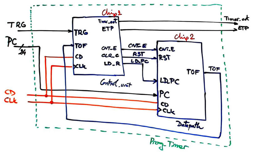
The aim of the project is to implement the control unit of the Prog_Timer circuit following automated design steps using VHDL techniques and CSD design conventions. When the state diagram of a FSM is known, its circuit realisation is synthesised using EDA tools effortlessly. As shown in Fig. 1, our FSM is Chip1 of P_Ch2 dedicated processor architecture. It advances using external control signals (TRG pulse) and internal status flags from the datapath (TOF flag) accordingly to the state diagram represented in Fig. 2.
  |
|
Fig. 1. FSM enmity under design. |
Fig. 2 shows the proposed state diagram for this FSM. It generates at each state the external timer outputs (Timer_out, ETP) and the internal control signals for running the datapath.
 |
|
Fig. 2. Proposed FSM state diagram. Black-coloured arrows (state transitions) are asserted at CLK's rising edges. |
Fig. 3 shows an example of timing diagram solved for a PC = 200. A timing period of TP = 12.5 μs is generated for a TCLK = 62.5 ns. Using the given parameters, a maximum timing period of about TP = 1 s is attained.
An interesting feature or enhancement can be added to Prog_Timer (in a new design phase) is an adjustable time scale, making the device able to time from ns to hours. We can run the datapath from another CLK source independently from the system CLK using a Chip3 CLK_Generator in the dedicated processor architecture and selecting time scales with a rotary switch.
 |
|
Fig. 3. Example of timing diagram. TRG signal last as long as the user is clicking the trigger button. If the trigger pulse duration is longer than the timing period, the state Trigger_check will last for many CLK periods until it goes down, meaning that the user has released trigger button, enabling the machine to perform another timing operation cycle. |
NOTE: Solve Lab6 and study tutorial projects in P6 before trying to solve this lab assignment.
2. Planning
Fortunately, once the system specified, from now on everything may be automated: pen and paper work following our CSD FSM design procedure.
a. Draw the general architecture of a finite state machine (FSM).
b. Adapt the general FSM architecture to this problem and draw the state register based on D_FF. Deduce how many D_FF are required if you are coding in binary sequential or in one-hot.
c. Write the truth table of CC1 and its equivalent behavioural interpretation in flowchart.
d. Write the truth table of CC2 and its equivalent behavioural interpretation in flowchart.
3. Developing
Using EDA tools for a target chip.
e. Write the VHDL file "Control_unit.vhd" by translating flowcharts and state register. Start a new project (Control_unit_prj) using an EDA synthesis tool for a CPLD MAXII EPM2210F324C or FPGA Cyclone IV EP4CE115F29C7. target chip.
f. Print and discuss the RTL schematic. Count the number of D_FF used in this application.
g. Print and discuss the technology view schematic. What is the difference in this final synthesised circuit when encoding states in binary sequential or in one-hot?
4. Testing (functional)
Using VHDL simulation tools.
h. Draw the testbench fixture for simulations and generate the file skeleton "Control_unit_tb.vhd"
i. Use the given testbench constant CLK_period in the CLK_process and stim_proc given in Fig. 4.
 |
|
Fig. 4. Testbench constant CLK_Period and an example of stimulus for testing a PC = 200. This is the VHDL translation of the activity represented in the Fig. 3 timing diagram. |
j. Start a functional simulation project using a VHDL testbench and discuss results. Fig. 5 shows an example on how to order signals and ports.
|
|
|
Fig. 5. Example of wave list and dividers to organise result in the logic analyser output. pay attention on how the internal FSM signals are represented to show current and next states. |

5. Testing (gate-level)
Using the same VHDL simulation testbench.
k. Start a gate-level simulation project and discuss results. Measure the tCO parameter for the selected target chip.
l. Measure the maximum CLK frequency that can be applied to your design using the timing analyser tool.
6. Report
Follow this rubric for writing reports. Because in this assignment you are solving one project, at least four sheets of paper are required.
| Home Term 23/24-Q2 Contact Products Electronic devices and companies Software Books Magazines Instruments DEE Library EETAC DEEL |

|
|
| Web activa des de 09/2001, @ F. J. Robert, J. Jordana. Web editat amb Microsoft Expression Web 4. El contingut és un complement als materials d'estudi del curs Circuits i Sistemes Digitals disponibles al campus digital Atenea. Llicència:Reconeixement 4.0 Internacional de Creative Commons |