|
|
Bachelor's Degree in Telecommunications Systems and in Network Engineering |
|
| | ||
P_Ch1: Designing arithmetic and logic circuits using hierarchical multiple-file plan C2 |
||
1. Specifications
The purpose of this project is to invent a chip capable of performing arithmetic operations. Fig. 1 shows the chip symbol and an example of input and output vectors when OP = "00". This project is aimed at Intel Cyclone IV EP4CE115F29C7 FPGA or MAX II EPM2210F324C3 CPLD target chips.
 |
Fig. 1. Arith_9bit unit to design and operations. |
-
Symbol and truth table represented in Fig. 1.
-
Deduce the operands range and practise with some example operations using different type of numbers. This is an example of operations to be performed by Arith_9bit and also a way to comprehend the meaning of the input vectors in context of the operation under execution (information or data processing).
This is the way Arith_9bit data must be interpreted when operating. Solve several operations of the circuit's truth table to comprehend correctly the data organisation.
 |
|
Fig. 2. Format of operands and results. |
-
Draw an example of timing diagram using Min_Pulse duration multiples as time reference.
EDA tools in use this semester to be installed in your portable computer after matriculating CSD: Intel Quartus Prime Lite, ModelSim Intel Edition, Proteus electrical simulator, minilog minimiser, notepad++ editor, Microchip MPLABX and XC8 compiler.
NOTE: For all projects, labs and tutorials, do not invent or change the name of a file, folder, component, signal, etc. that are given in schematics, diagrams or explanations. All the names and features are carefully selected and annotated to make it easy to solve projects in the given study time. If you have the need to invent a name, for instance to translate to VHDL a plan C2 circuit, do not do it, but ask questions instead in order to get help and solve your doubts. This is our way to save you countless unproductive hours.
NOTE: Be aware that these projects are only semi-structured, organised in a way to encourage you to ask countless questions as long as you go along.
2. Planning
Planning several design phases (subprojects):
| Due date March 8 | Circuit analysis using Proteus and Wolfram Alpha |
|
March 15 | Circuit analysis using VHDL tools |
|
March 22 | Circuit design using single-VHDL file plans A and B |
|
April 1 | Circuit design using hierarchical plan C2 |
|
P_Ch1 |
April 1 | Report, video and project files | Q & A |
Key note: Only materials submitted before due dates are considered for grading. To avoid any problems with file types or sizes, please, do not wait until the last minute. And be sure that your files can be downloaded and unzipped correctly and also that there is a clear link to your video presentation. Add as well your own self-assessment indicating what grade you might get with respect to the marking grid.
Project location:
C:\CSD\P_Ch1\Arith_9bit\
This chip can be designed internally using many strategies. To make it simple, we propose a given architecture represented in Fig. 3 based on a hierarchical structure of components and signals. Chip1 is a 9-bit selectable adder subtractor to work with radix-2 and integer numbers for performing "00", "10" an "11" operations. Chip2 is a radix-2 9-bit comparator for performing "01" operation. Plan and develop Chip1, Chip2 and Chip3 before building the top entity.
 |
|
Fig. 3. Top level internal architecture for the Arith_9bit. |
Thus, you better follow this sequence to complete the lab project:
1) Invent Chip2 component Comp_9bit as stated in the assignment SP1_4.
Learning how to translate to VHDL a plan C2 circuit composed of multiple components and signals is, again, the key issue. Therefore, this is a new video rec. on Adder_2bit from SP1_3 using now plan C2 that is of your interest.
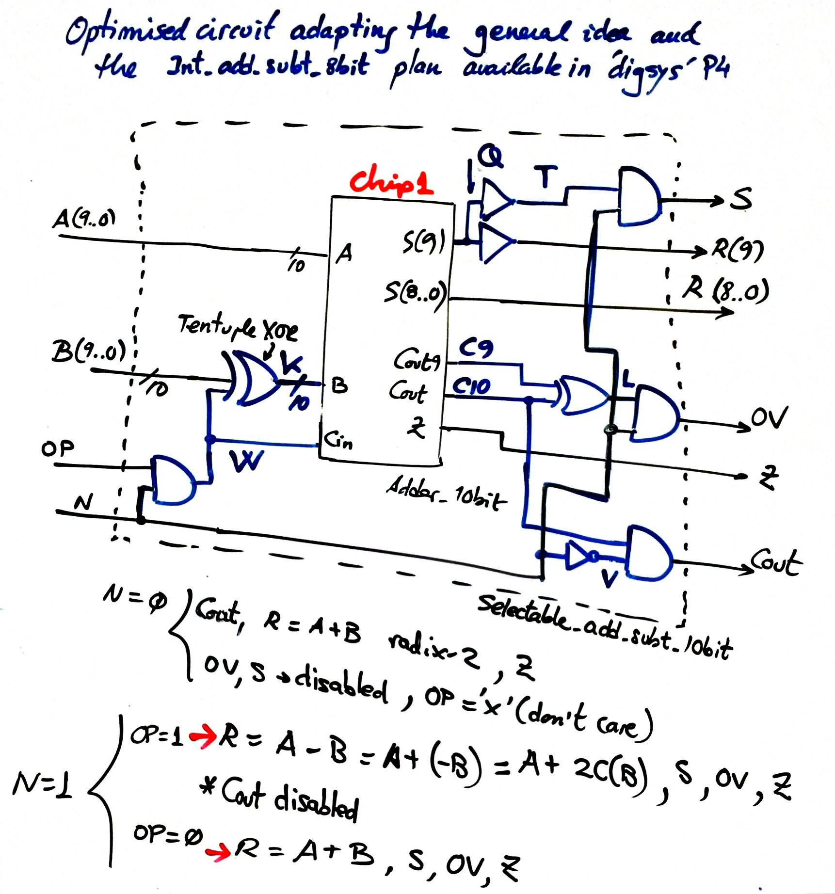
2) Invent Chip1 component Sel_Add_Subt_9bit using hierarchical architectures similar to P3 and P4.
Fig. 4 below shows you some ideas and planning. One option is to build the component Adder_9bit using materials from P3. Pay attention that now you must include Cout8 as a port to be able to generate overflow (OV) flag function.
 |
|
Fig. 4. Ideas on how to organise Chip1. |
More ideas from former project Selectable_add_subt_12bit circuit. Input N decides what data type to add or subtract: radix-2 or integer numbers. Conceptual idea on designing a circuit for several operations, a plan and video rec. on how to translate such plan into a VHDL equivalent file for developing the project.
3) Invent Chip_3 component. You can choose plan C2 or plan B for the Triple_MUX_2.
4) Assemble all the blocks, develop and test the complete Arith_9bit. Run several operations from its truth table to demonstrate that it works as expected.
3. Developing
The development of P_Ch1 implies completing each component beforehand and the final construction in VHDL of the circuit in Fig. 3.
Translate to VHDL the plan in Fig. 2 and write the Arith_9bit.vhd. Run a synthesis project for the target chips: MAX II EPM2210F324C3 or Cyclone IV EP4CE115F29C7.
Examine and discuss RTL and technology schematics. Determine how many resources are used for building this project Arith_9bit.
Testing P_Ch1 implies testing some components beforehand and the final verification of the circuit in Fig. 3 using several test vectors and operations.
Organise a VHDL testbench Arith_9bit_tb.vhd.
Run a ModelSim functional simulation and examine results from logic analyser to determine whether the circuit works as expected. To check and veryfy how the circuit works, you can use four pictures like the one presented in Fig. 5 for testing operation "00".
 |
|
Fig. 5. Example of expected waveform for operation OP = "00". For this operation A, B are unsigned radix-2 numbers. As studied in these examples, the same combinations A and B can be used for other operations but has to be interpreted accordingly to the data type selected. |
Marking grid
| Work in progress assessments to be carried out in laboratory sessions (individual) | ||||
| SP1_1 | SP1_2 | SP1_3 | ||
| 1p | 1p | 1p | ||
Note Work in progress includes completing tutorials, sample reports, sketches, diagrams, discussions, Q & A, presentations, live demonstrations, results, measurements, etc.
| P_Ch1 handwritten report and video presentation (group): | |||||
| SP1_1 | SP1_2 | SP1_3 | SP1_4 | Video | P_Ch1 |
| 1p | 1p | 1p | 1p | 1p | 2p |
Notes on lab assessment: student grades are not simply reflecting report or video quality, but implicitly, they include laboratory attendance and punctuality, participation, Q & A, problem solving skills, active attitude and group work.
Follow this rubric for writing reports. Because in this assignment you are solving two projects, at least eight sheets of paper are required.
Notes on how to write and organise your report
Report layout. Example of P_Ch1 written report layout (one submission per cooperative lab group), a single PDF file:
1. Specifications and theory
Original handwritten materials on symbol, truth table, timing diagram and other explanations on data types and operations to be performed.
2. Planning
Original handwritten explanations and VHDL-ready schematics on how this plan C2 circuit is conceived, the proposed hierarchy of components, signals, number of VHDL files, project folders and names, etc.
3. Development
Project in Quartus Prime for a target FPGA chip: Intel Cyclone IV EP4CE115F29C7. Printings and handwritten discussions of RTL and technology schematics. How many FPGA resources (logic cells, logic elements, etc.) are used?
4.Test and verification
Testbench schematic, proposed stimulus testbench process. Printings and handwritten discussions on results.
Add your conclusions on the project done and on what has been learned. Remember that your self-assessment is expected to be submitted as well at the Atenea platform.
5. Annexes
Add here work done in previous weeks and assessed in work in process.
- A1 (SP1_1 on learning analysis methods I and II)
It may be a group submission that includes improvements from feedback and corrections on SP1_1 materials discussed during lab work assessments.
- A2 (SP1_2 on learning analysis method IV)
It may be a group submission that includes improvements from feedback and corrections on SP1_2 materials discussed during lab work assessments.
- A3 (SP1_3 on learning design plans A and B)
It may be a group submission that includes improvements from feedback and corrections on SP1_3 materials discussed during lab work assessments.
- A4 (SP1_4 on learning design plan C2)
It may be a group submission, this is your first submission of SP1_4: project organised as (1) - (2) - (3) - (4) like all the other projects.
- A5 Other materials or components you like to include.
Notes on video presentations: 10 min. max., 3 -4 min. each participant.
The idea of the video presentation is different from the report and has its own particular objective: develop your oral communications skills in this engineering context.
No need to explain every single detail of every project or exercise you have been solving for more than a month, but start putting in motion your communication skills that you will continue to practise and improve through P_Ch2 and P_Ch3.
Therefore, you can choose something to explain: a component, a subproject, or the complete Arith_9bit in P_Ch1, because we will focus assessment in how you are organising the presentation, how confident you are in front of the camera, time sharing among students, support materials, time distribution and audio and video quality.
| Home Term 23/24-Q2 Contact Products Electronic devices and companies Software Books Magazines Instruments DEE Library EETAC DEEL |

|
|
| Web activa des de 09/2001, @ F. J. Robert, J. Jordana. Web editat amb Microsoft Expression Web 4. El contingut és un complement als materials d'estudi del curs Circuits i Sistemes Digitals disponibles al campus digital Atenea. Llicència:Reconeixement 4.0 Internacional de Creative Commons |