|
|
Bachelor's Degree in Telecommunications Systems and in Network Engineering |
|
|
|
|||||
Chapter 3 problems |
- D3.6 - |
-- 7-segment digit sequencer (μC - C version) |
|||
|
|
|||||
1. Specifications
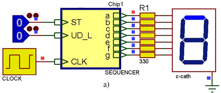
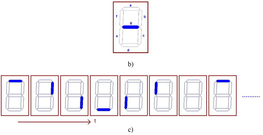
We want to design a simple driver to shown a sequence of movement, clockwise and counterclockwise, in a single 7-segment display using a PIC18F microcontroller. Fig. 1 represents the schematic diagram of the application. The same circuit was already proposed as a FSM in problem: D2.6.
The circuit components are: (1) a clock to produce a rectangular wave with a given frequency, let us take for instance 5 Hz; (2) the digital system named sequencer and (3) the 7-segment display (common cathode) with its current-limiting resistors.
Switch UD_L = '1', clockwise; UD_L = '0', counterclockwise
  |
|
Fig. 1. a) Block diagram of the circuit. b) Digit segments and position when idle. c) Sequence of switching LED segments for UD_L = '1' (clockwise, up counting). |
The system has to work as specified in Fig. 1c, depending on the logic levels of the synchronous input signals: UD_L (Up, active high / Down, active low) and start/stop button (ST). A start ST pulse activates the sequence of digit rotation that never ends until another pulse ST is applied and the sequence has reached the last state.
Some questions to kick off the project and organise it the usual four sections and also considering our step-by-step design approach introducing a new feature at a time.
- Step #1: Basic project simply rotating in only one direction.
- Step #2: Make it bidirectional introducing UD_L
- Step #3: Add the ST feature.
Step #1:
a) Draw the hardware schematic necessary for step #1. CLK push button or oscillator, outputs a, b, c, d, e f, g, reset circuit MCLR_L, and an 8 MHz quartz crystal oscillator. Explain how to configure the inputs and outputs in init_system().
b) Draw the function table and the state diagram indicating state transitions and outputs.
c) Draw the hardware/software diagram indicating the required RAM variables and how the FSM is solved in software.
d) Draw the truth tables and their equivalent flowcharts for state_logic() and output_logic() functions.
e) What is the interrupt service routine ISR() used in this application? Draw its flowchart.
f) Develop and test (debugging) the project capturing the hardware circuit in Proteus and writting the C source code.
Step #2:
a) Draw the hardware schematic necessary for step #2. Add the switch and resistor for input UD_L. Explain how to configure it in init_system().
Similar b), c), d), e)
Step #3:
a) Draw the hardware schematic necessary for step #3. Add the pushbutton ST switch and resistor for input ST. Explain how to configure it in init_system().
Similar b), c), d), e)
Design phase #2:
Let us add an LCD display to this application. The idea is to use several characters to represent an equivalent sequence.
g) Enhance the schematic from design phase #1 to include an LCD attached to port D as studied in tutorials.
h) Enhance the software and the source file to drive the LCD.
In this design phase also two design steps may be conceived, for instance:
- step #1: Print ASCII messages on the LCD.
- step #2: Print as well the number of rotations (dynamic numerical data).
Design phase #3:
The external CLK is replaced by the internal 8-bit TMR2 peripheral to generate interrupts (TMR2IF).
i) Calculate TMR2 parameters required to generate a CLK of 5 Hz (var_CLK_flag period = 200 ms) to run the machine.
j) Add a new switch SP (speed) to be able to select between two different rotation periods: 200 ms and 100 ms.
| Home Term 23/24-Q2 Contact Products Electronic devices and companies Software Books Magazines Instruments DEE Library EETAC DEEL |

|
|
| Web activa des de 09/2001, @ F. J. Robert, J. Jordana. Web editat amb Microsoft Expression Web 4. El contingut és un complement als materials d'estudi del curs Circuits i Sistemes Digitals disponibles al campus digital Atenea. Llicència:Reconeixement 4.0 Internacional de Creative Commons |