|
|
Bachelor's Degree in Telecommunications Systems and in Network Engineering |
|
|
|
|||||
Chapter 2 problems |
- D2.12 - |
Electronic roulette |
|||
|
|
|||||
1. Specifications
Let us design an electronic roulette as shown in Fig. 1. After turning on the power supply, a 3.3 V battery, the roulette inicialises showing number 0 (yellow LED). The circuit keeps the last bet LED lighting. While clicking the play (P_L) button the wheel is spinning and when the button P_L is released a new bet is shown. Let us invent this circuit using plan C2 and proposing a dedicated processor [8.1] architecture for counting and controlling the play button.
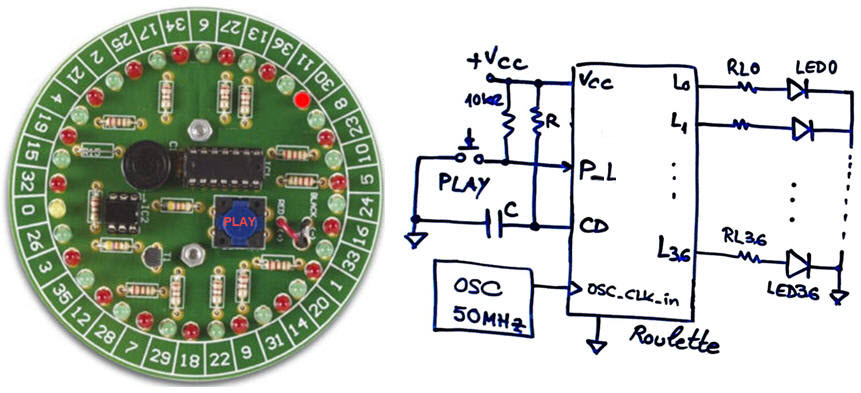 |
| Fig. 1. Electronic roulette. The wheel have a zero (house edge), and numbers from 1 to 36. The odds of winning are thus 37 to one (2.7%). |
Fig. 1 shows the symbol of the top schematic Roulette. Now it is time to imagine how the circuit may work in time as an standard Chapter 2 circuit, with button detection and code generation.
Sketch a timing diagram showing how the circuit operates. The Fig. 2 is a first example. We assume option CLK #1 values, we imagine that in a first design the LED spin at the same frequency for generating a random number.
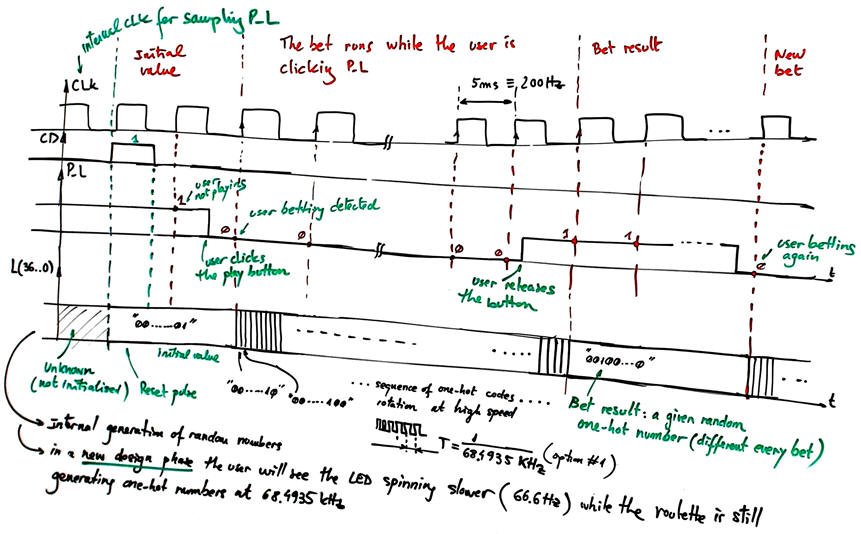 |
| Fig. 2. Example of initial timing diagram. While betting the one-hot numbers (only one LED lighting at a time and rotating) are generated at a large weird frequency. Alternatively to start the project, and because the CLK_genentor is not yet designed, we can imagine that the numbers are also generated at 200 Hz, the CLK for sampling the play button. |
Thus, the project continues planning the Datapath, the CLK_Generator and the FSM components of the dedicated processor.
Optional design phase #2. After three minutes of not touching P_L, the machine generates a sequence of LED in movement, to show that it is active and waiting for the user to play. Thus the circuit keeps the last bet LED lighting only for three minutes.
Plan option #1. BCD counting
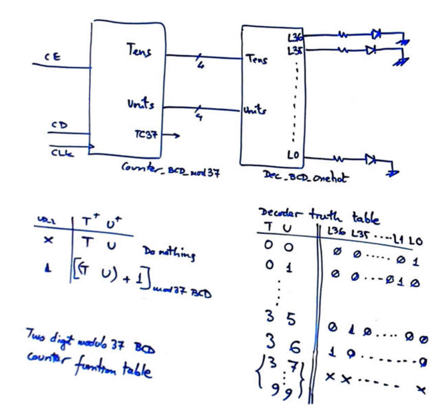
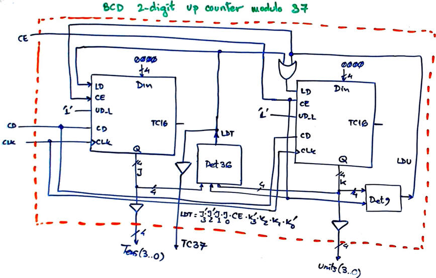
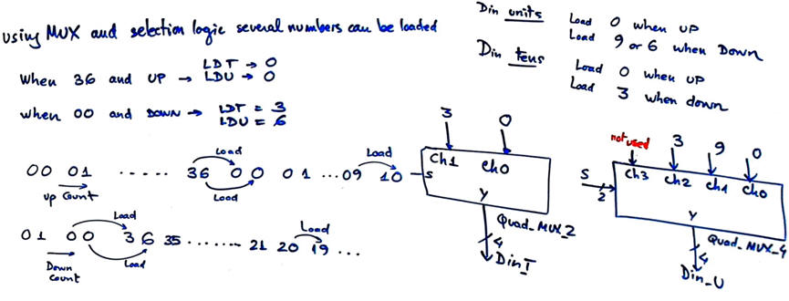
Let us design a synchronous two digits BCD modulo 37 [00, 01, 02, ..., 09, 10, 11, ..., 36, 00, 01, ...] up counter. We will follow structural VHDL plan C2 using EDA tools and counter chaining and truncation techniques. The building block for counting is our Counter_mod16 and other combinational components and logic. A decoder will be required to translate BCD to one-hot code for driving high the 37 LED. Fig. 3 and Fig. 4 may help you. CE and CD may be controlled by a FSM driven by the roulette play (P_L) button that has to generate BCD codes while kept clicked.
 |
|
Fig. 3. Ideas on how to count in BCD and decode to one-hot. How to build a Dec_BCD_onehot component using standard components from other CSD libraries or projects? |
  |
|
Fig. 4. The idea of a BCD counter modulo 37 and the logic behind count truncation. A similar example is studied in P7 highlighted project on an Hour_counter (BCD counter modulo 24) |
Plan, develop and test the datapath and the FSM. Write the VHDL files and start an EDA project to synthesise the circuit for an FPGA target chip and obtain results. Inspect the RTL and verify that it looks like your schematic. Check the number of D_FF used in this application, print and comment the schematics. Write a VHDL test bench and run the EDA simulation tool to verify your design.
Plan and add the CLK_generator [8.2] to the previous circuit to run the application with a CLK squared signal of 68493.5 Hz derived from the 50 MHz crystal oscillator. Users see the wheel of LED is spinning while the play button P_L is kept pressed; turning on and off all the 37 LED takes about 1.8 s (66.6 Hz squared waveform).
In case that the play button sampling frequency is too high, we can generate another one, such 200 Hz as we did in other applications based on buttons and keys.
Project location:
C:\CSD\P7\roulette1\(files)
Plan option #2. Binary radix-2 counting
Similar to provious option 1 but counting in radix-2. Use as well the building block Counter_mod16 for counting.
Plan, develop and test the datapath and the FSM. Write the VHDL files and start an EDA project to synthesise the circuit for an FPGA target chip and obtain results. Inspect the RTL and verify that it looks like your schematic. Check the number of D_FF used in this application, print and comment the schematics. Write a VHDL test bench and run the EDA simulation tool to verify your design.
Plan and add the CLK generator [8.2] to the previous circuit to run the application with a CLK squared signal of 2173913 Hz derived from the 50 MHz crystal oscillator. Users see the wheel of LED is spinning while the play button P_L is kept pressed; turning on and off all the 37 LED takes about 1.2 s (44.4 Hz squared waveform).
In case that the play button sampling frequency is too high, we can generate another one, such 200 Hz as we did in other applications based on buttons and keys.
Project location:
C:\CSD\P7\roulette2\(files)
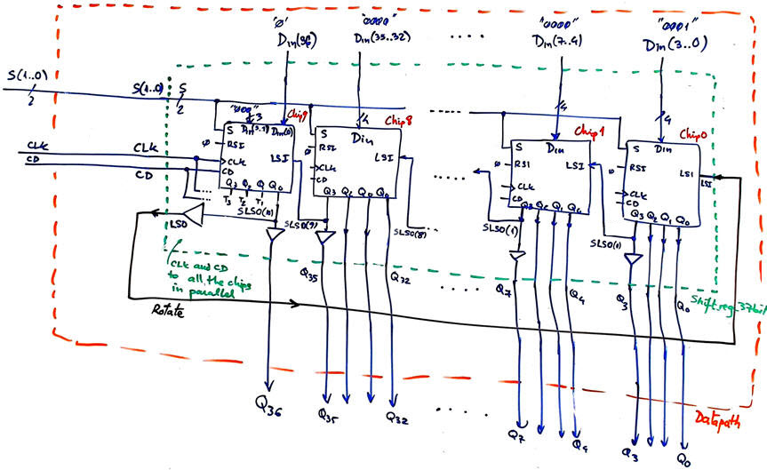
Plan option #3. Shift registers and bit rotation
Invent, develop and test the datapath and the FSM for this application. The datapath includes shift registers components such Shift reg_4bit connected to expand to 37 LED and also allow bit rotations.
For example, Fig. 5 shows how a 37-bit shift register can be invented for this specific datapath where only a left rotation of an initial value (37-bit one-hot code) is necessary.
 |
|
Fig. 5. The idea of a datapath based on shift-registers and (left) bit rotation. This datapath may be used while betting (keeping pressed the play button). It yet has to be modified for showing as well the wheel of LED spinning at a much lower speed. |
A good question now, even if it is beyond what is required in this roulette, is how to build a full featured 37-bit shift register (left and right bit shifting) using the same plan C2 in Fig. 5.
Users see de wheel of LED is spinning while the play button P_L is kept pressed; turning on and off all the 37 LED takes about 1.5 s (55.5 Hz squared waveform). We can try to run both, the FSM for sampling the play button and the datapath clocked at very high speed, for instance, 555555.555 Hz. Design the CLK generator [8.2].
In case that the play button sampling frequency is too high, we can generate another one, such 200 Hz as we did in other applications based on buttons and keys.
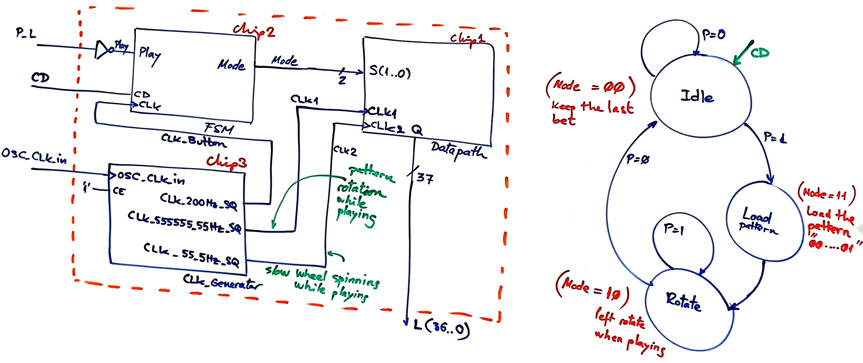
Fig. 6 represents a top schematic for the dedicated processor imagining that the button sampling speed is 200 Hz, the playing speed is 555555.555 Hz, and that the wheel is spinning at low speed (55.5 Hz) to show the user that the roulette is working.
 |
|
Fig. 6. Example dedicated processor showing how to CLK frequencies for different purposes. The picture includes an example state diagram for the FSM in control of the datapath. |
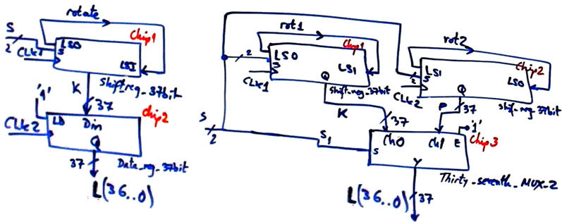
The final design of the datapath, as shown in Fig. 7, may be decided once the prototype is running. In one version, the Chip2 Data_reg_37bit is subsampling at 55.5 Hz the current rotating value. In the other version, the rotator circuit is duplicated, each one working at a different frequency; when playing the slow rotator connected to CLK2 is displayed.
 |
|
Fig. 7. Alternative datapath designs. |
Project location:
C:\CSD\P7\roulette3\(files)
| Home Term 23/24-Q2 Contact Products Electronic devices and companies Software Books Magazines Instruments DEE Library EETAC DEEL |

|
|
| Web activa des de 09/2001, @ F. J. Robert, J. Jordana. Web editat amb Microsoft Expression Web 4. El contingut és un complement als materials d'estudi del curs Circuits i Sistemes Digitals disponibles al campus digital Atenea. Llicència:Reconeixement 4.0 Internacional de Creative Commons |