|
|
Bachelor's Degree in Telecommunications Systems and in Network Engineering |
|
|
|
|||||
Chapter 2 problems |
- D2.1 - |
CD player controller |
|
||
|
|
|||||
1. Specifications
Our aim is to design a CD player controller based on sampling the control buttons and switches available on the front panel following our FSM strategy. This is a design projet in five sections.
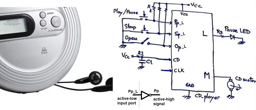 |
| Fig. 1. CD player application and its symbol. |
Learn form our tutorials in LAB6, P6 and other tutorial projects on FSM how the idea of sampling buttons works. A convenient CLK signal for sampling buttons may be 200 Hz.
Draw an example of timing diagram (for example considering only the control signal in the design phase #1 bellow)
Can you find commercial devices where similar buttons control how the music is played (Hi-Fi audio chain, Bluetooth earbud, DVD player, etc.)? What button is the most important?
NOTE: The idea is to read and study as much as you like materials, books, examples or advanced tutorials, but do not copy from them. Your aim is to imagine that this project is derived from the LAB6 tutorial where we organised a FSM controlled clicking a single button. The better you comprehend the laboratory tutorial the faster will you design this application.
2. Planning ideas and options
The planning is based on applying our FSM recipe. This architecture is translated to VHDL as a plan C1 single file where the three main components are processes.
Imagine several design phases to conceive and complete the full project. For instance:
- Design phase #1: Player with a single button Play/Pause.
Project location:
C:\CSD\P6\CD_player1\(files)
Therefore, only when this phase #1 is complete and functionally working (1-2-3-4),
- Design phase #2: Player with buttons Play/Pause and Stop and also with the door switch Open.
Project location:
C:\CSD\P6\CD_player2\(files)
And here, you can add the section 5
Propose a state diagram.
 |
| Fig. 2. CD player FSM state diagram for design phase #1. |
Adapt the FSM architecture to this problem, naming and connecting all signals and inputs and outputs.
Deduce how many D_FF are required when encoding FSM states using the following options and draw the state register memory:
Option #1: radix-2 (sequential)
Option #2: Gray
Option #3: Johnson
Option #4: one-hot
Draw the state register memory block.
Write the truth table of CC2 and CC1 and their equivalent behavioural interpretations (plan B) using flowcharts.
Write the FSM VHDL file.
Start a Quartus Prime synthesis project for one of the following programmable target chips:
Option #1: Cyclone IV EP4CE115F29C7
Option #1: MAX II EPM2210F324C3
Inspect and annotate the RTL and technology views. Check the number of D_FF synthesised in this application.
Generate a VHDL testbench fixture schematic. Translate the timing diagram sketch from the specifications into de corresponding stimulus processes.
Run functional simulations to verify your design. Visualise as well in the wave timing diagram the internal states.
Run gate-level simulations to measure the propagation time CLK to output (tCO). Measure the minimum TCLK period or the maximum frequency of operation of the FSM.
Optional additional circuit when P8 content is comprehended. Design the CLK generator circuit from a 50 MHz quartz crystal oscillator to obtain the 200 Hz CLK signal. Deduce the number of D_FF that it will contain. Build a prototype for the DE10-Lite board assigning pins and uploading the configuration file to the FPGA.
| Home Term 23/24-Q2 Contact Products Electronic devices and companies Software Books Magazines Instruments DEE Library EETAC DEEL |

|
|
| Web activa des de 09/2001, @ F. J. Robert, J. Jordana. Web editat amb Microsoft Expression Web 4. El contingut és un complement als materials d'estudi del curs Circuits i Sistemes Digitals disponibles al campus digital Atenea. Llicència:Reconeixement 4.0 Internacional de Creative Commons |