|
|
Bachelor's Degree in Telecommunications Systems and in Network Engineering |
|
|
|
|||||
Chapter 1 problems |
- D1.1 - |
Wind compass |
|
||
|
|
|||||
1. Specifications
We want to design a digital wind direction meter (wind_compass) as shown in Fig. 1, based on a 16-position optoelectronic rotary encoder. Discuss using handwritten comments the RTL and the technology schematics. How many logic elements are used? The synthesised circuit will be tested using VHDL testbenches.
To promote class and cooperative group discussions, we can plan the project in several ways, as represented in our CSD design flowchart. Each plan means a different project and circuit realisation that is useful for comparing solutions.
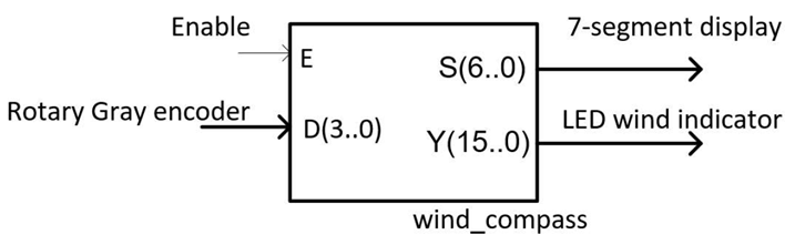 |
| Fig. 1. Circuit symbol and its realisation in Proteus wind_compass.pdsprj for better comprehending how does it work. As with many more designs, the same project is proposed in A3.1 to be solved using a microcontroller in Chapter 3. |
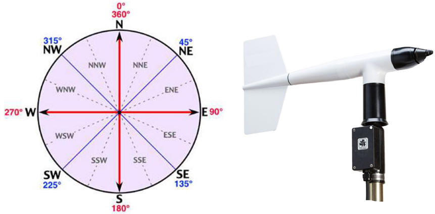
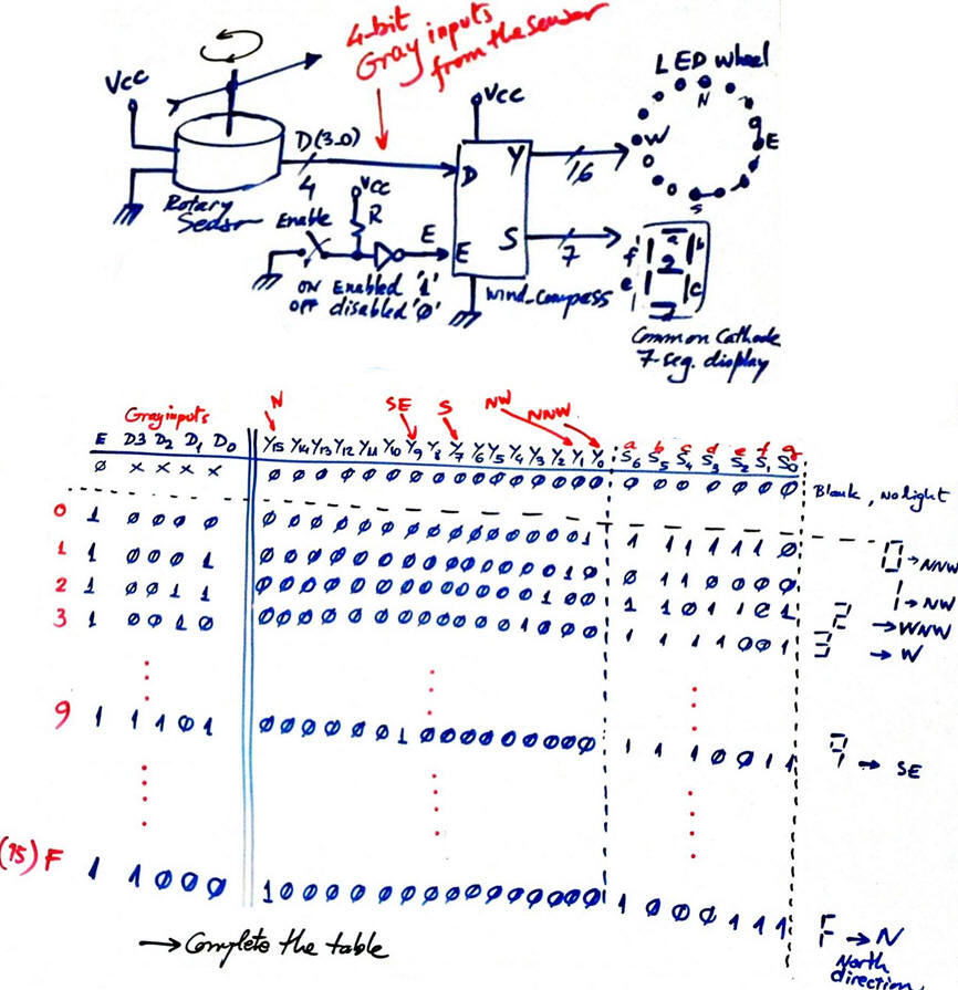
Fig. 2 represents the wind compass subdivided in 16 directions each of which is assigned to a 4-bit Gray code.
 |
|
Fig. 2. Wind compass describing the sixteen principal bearings used to measure wind direction and an example of commercial manufactured wind transducer. |
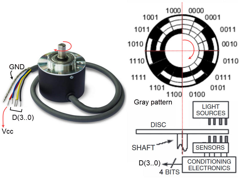
Fig. 3 represents the sensor disk coded in Gray, which is used instead of binary radix-2 code to prevent spurious outputs from electromechanical switches. The objective is to develop the VHDL code and the final circuit to be synthesised into a target complex programmable device (CPLD) or a field programmable gate array (FPGA) chip.
 |
|
Fig. 3. Gray code error reduction with encoders (ref.) Adjacent codes differentiate themselves by only one bit which makes this codign style very convenient for a rotating wheel. |
 |
|
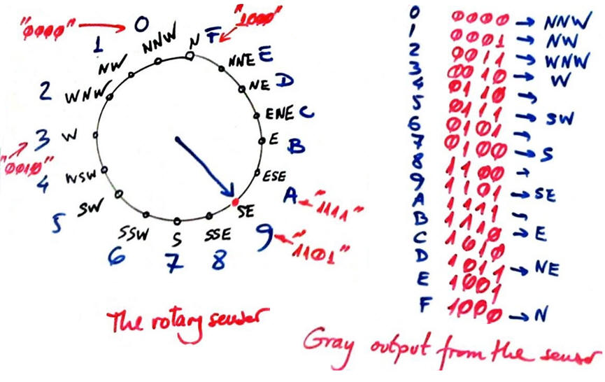
Fig. 4. Sensor codes assigning for instance the code "0000" to the NNW direction. |
Write the truth table of the wind_compass. The inputs have to be ordered in this way: E, D(3..0).
 |
|
Fig. 5.Wind compass circuit and truth table. |
Draw an example timing diagram showing the input stimulus and output responses. Assuming that Min_Pulse = 3.56 ms, how long does it take to simulate all the circuit specifications?
CPLD or FPGA target chip options:
option #1.: MAX II
option #2.: MAX 10
option #3.: Cyclone IV
Planning
Plan A: Structural design in a single VHDL file (flat), using logic equations in canonical or minimised versions. For instance:
option #1:
- Write the functions Y(7) and Y(14) canonically as a product of maxterms.
- Write the functions S(6) and S(1) canonically as a sum of minterms.
- Write the functions S(2) and Y(13) as an SoP and draw the equivalent logic circuit.
- Write the functions S(0) and Y(11) as a PoS and draw the equivalent logic circuit.
- Write the functions S(4) and Y(5) using only NOR2.
- Write the functions S(3) and Y(10) using only NAND.
Project location:
C:\CSD\P2\wind_compass\planA1\(files)
option #2:
- Write the functions Y(7) and Y(14) canonically as a sum of minterms.
- Write the functions S(6) and S(1) canonically as a product of maxterms.
- Write the functions S(2) and Y(13) as a PoS and draw the equivalent logic circuit.
- Write the functions S(0) and Y(11) as a SoP and draw the equivalent logic circuit.
- Write the functions S(4) and Y(5) using only NAND2.
- Write the functions S(3) and Y(10) using only NOR.
Project location:
C:\CSD\P2\wind_compass\planA2\(files)
Plan B: Behavioural flat design with a single VHDL file, using high-level description of the specifications.
Draw a schematic to translate the wind_compass truth table to VHDL, representing the required signals to interface the truth table artefact.
Project location:
C:\CSD\P2\wind_compass\planB\(files)
Plan C2: Structural hierarchical design with multiple VHDL files, building the project using an architecture consisting of components and signals.
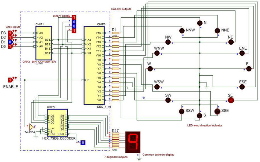
Fig. 6 shows an example of an internal electronic schematic for the wind_compass when plan C2 is used. It is available for experimentation wind_compass.pdsprj. The output of Chip1 (Gray_bin_converter) is connected to both Chip2, a 1-digit 7-segment decoder (HEX_7seg_decoder), and Chip 3, a 16-bit decoder (Dec_4_16) with one-hot output to light a wheel of 16 LED to display the wind direction.
 |
|
Fig. 6. Internal design for the project wind_compass based on plan C2. The picture shows the Gray code "1101" that is "1001" in binary radix-2 representing the wind direction South-East "SE". In the way it is connected, the code "0000" corresponds to the direction "NNW", and it advances counter-clockwise up to the code "1111"which is the direction "N". |
Run the Proteus simulator of the circuit in Fig. 6. Print the screen results when you input the Gray code "0101" and explain how it works.
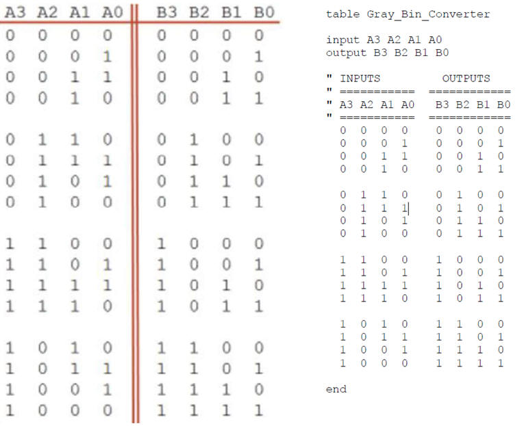
Fig. 7 shows the Chip1 truth table. Realise how the 16 input combinations do not have to be ordered necessarily in binary radix-2.
 |
|
Fig. 7. Chip1 Gray_bin_converter truth table to be written to minilog for extracting its equations. |
Project location:
C:\CSD\P2\wind_compass\planC2\(files)
After having studied P4 tutorials, additional questions can be added to our report. For instance:
-
Perform a gate-level simulation to measure propagation delays in a given signal transition.
-
Deduce the worst-case propagation delay running the timing analiser tool and calculate the circuit's maximum frequency of operation for the target chip used in the design.
-
In the end, because three alternative circuits are proposed for the wind_compass, we can compare which one is faster and which one uses less resources (logic elements).
| Home Term 23/24-Q2 Contact Products Electronic devices and companies Software Books Magazines Instruments DEE Library EETAC DEEL |

|
|
| Web activa des de 09/2001, @ F. J. Robert, J. Jordana. Web editat amb Microsoft Expression Web 4. El contingut és un complement als materials d'estudi del curs Circuits i Sistemes Digitals disponibles al campus digital Atenea. Llicència:Reconeixement 4.0 Internacional de Creative Commons |